Solar Cell of Anti Potential Induced Degradation and Manufacturing Method Thereof

a solar cell and potential degradation technology, applied in the field of solar cell manufacturing, can solve the problems of prone to potential degradation, leakage current, and passage of current between glass substrate and package material, and achieve the effect of improving the electrical performance of the photovoltaic module and good electrical insulation property

Inactive Publication Date: 2014-09-25
JINKO SOLAR CO LTD
View PDF4 Cites 8 Cited by
  • Summary
  • Abstract
  • Description
  • Claims
  • Application Information

AI Technical Summary

Benefits of technology

[0006]In order to solve the above-mentioned technical problem, a solar cell of anti potential induced degradation and a manufacturing method thereof are provided according to embodiments of the invention. The solar cell manufactured by using the manufacturing method has a good electrical insulation property with outside packaging material and the glass substrate, so the corresponding photovoltaic module has an anti potential induced degradation effect, which improves the electrical performance of the photovoltaic module operating under the high negative voltage for a long time.
[0022]Compared with the prior art, the above-mentioned technical solutions have the following advantages.
[0023]According to the technical solutions provided by the embodiments of the invention, the plasma cleaning is firstly performed on the silicon wafer by using the oxidizing gas, so as to form a compact first silicon oxide film on the surface of the silicon wafer while cleaning the silicon wafer; then the anti-reflection film is formed on the surface of the cleaned silicon wafer, i.e., the anti-reflection film is formed on the surface of the first silicon oxide film, where the anti-reflection film includes at least a silicon oxide film. Since the silicon oxide film has a good electrical insulation property and an anti-reflection effect, the solar cell manufactured by using the manufacturing method provided by the embodiments of the invention has a good electrical insulation property with the packaging material and the glass substrate, so the corresponding photovoltaic module has an anti potential induced degradation effect, which improves the electrical performance of the photovoltaic module operating under the high negative voltage for a long time.

Problems solved by technology

However, in the photovoltaic module manufactured by using the existing solar cell manufacturing processes, a potential induced degradation (referred to as PID for short) effect is prone to occur.
That is, the photovoltaic module operates under a high negative voltage for a long time, so there will be a leakage current passage between the glass substrate and the package material.
Therefore, a large number of charges are accumulated on the surface of the solar cell, and the charges accumulated on the surface of the solar cell may draw photogenic charge carriers, leading to leakage current.
Therefore, electrical performance parameters of the photovoltaic module, such as the fill factor FF, the short circuit current Jsc and the open circuit voltage Voc are deteriorated, and thus the electrical performance of the photovoltaic module will be lower than the design criteria.

Method used


Image

  • Solar Cell of Anti Potential Induced Degradation and Manufacturing Method Thereof
  • Solar Cell of Anti Potential Induced Degradation and Manufacturing Method Thereof
  • Solar Cell of Anti Potential Induced Degradation and Manufacturing Method Thereof

Examples


first embodiment

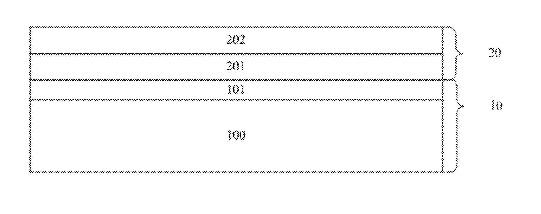
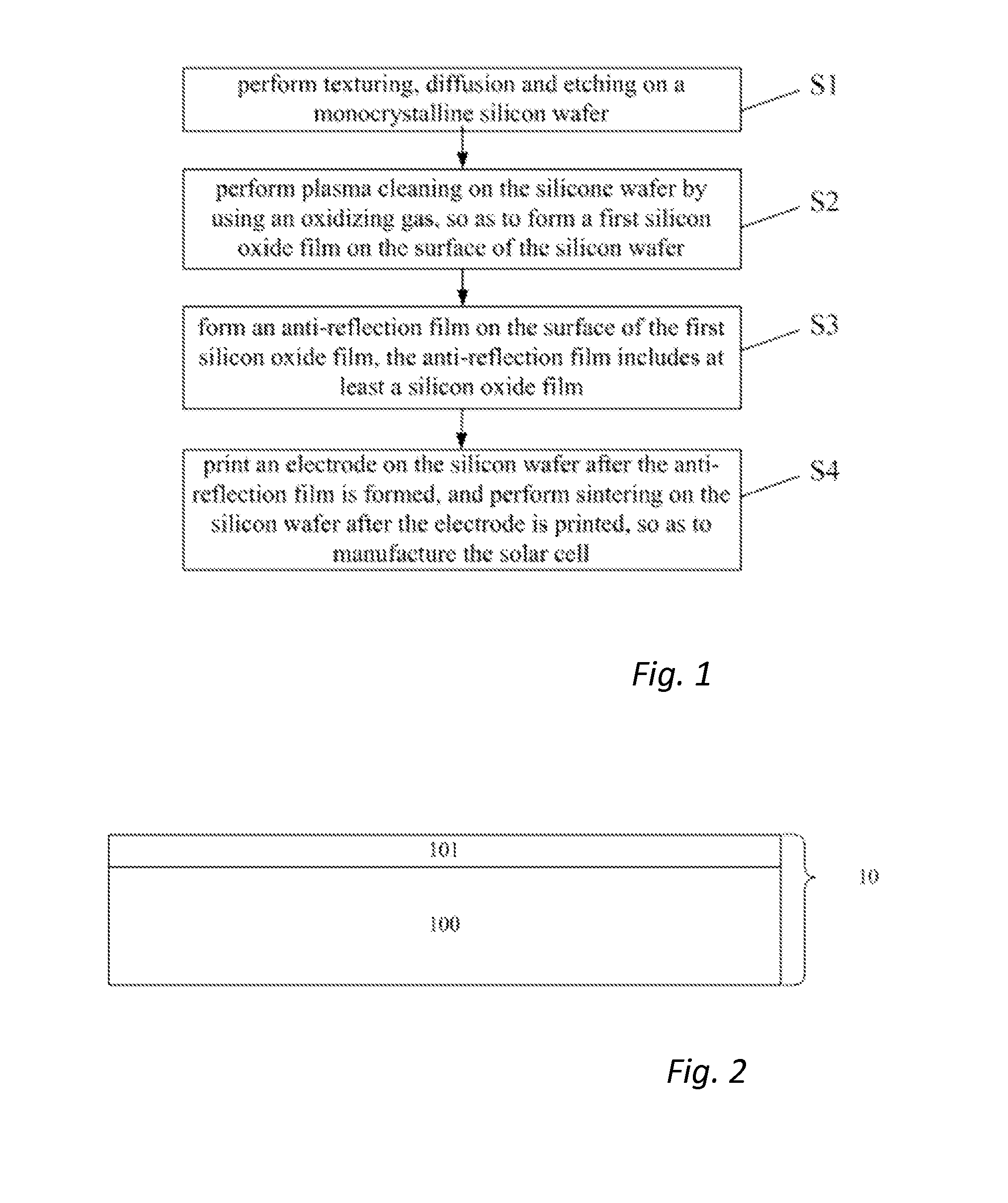
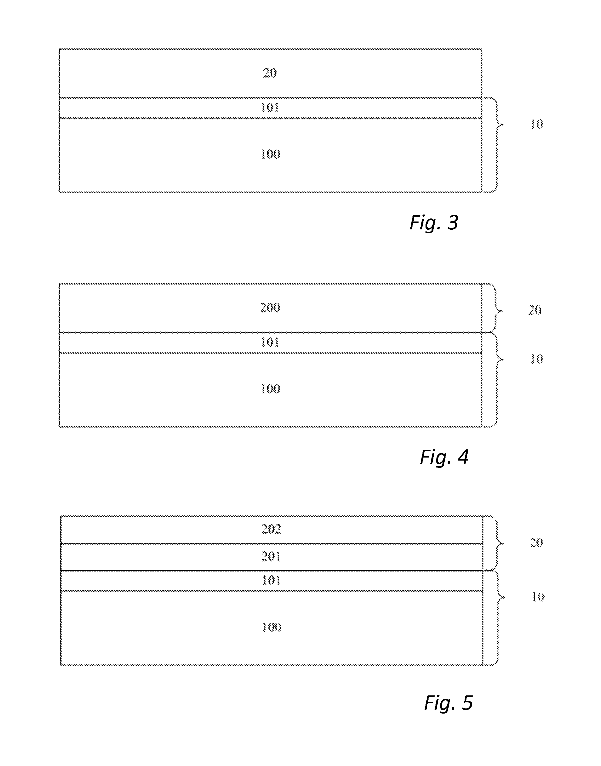
[0038]As shown in FIG. 1, a method for manufacturing a solar cell is provided by an embodiment of the invention, including the following steps.

[0039]Step S1: performing texturing, diffusion and etching on a monocrystalline silicon wafer. It should be noted that the monocrystalline silicon wafer may be a P-type monocrystalline silicon wafer or an N-type monocrystalline silicon wafer, and it is not limited in the present invention. In the embodiment of the invention, the method for manufacturing the solar cell provided by the invention is described in detail by using the P-type monocrystalline silicon wafer as the monocrystalline silicon wafer as an example. Thus, in an embodiment of the invention, the performing texturing, diffusion and etching on a monocrystalline silicon wafer includes performing acid texturing, phosphorus diffusion and etching on a P-type monocrystalline silicon wafer.

[0040]Step S2: performing plasma cleaning on the silicon wafer by using an oxidizing gas, so as t...


PUM

PropertyMeasurementUnit
thicknessaaaaaaaaaa
thicknessaaaaaaaaaa
thicknessaaaaaaaaaa

Abstract

A solar cell of anti potential induced degradation and a manufacturing method thereof are disclosed by embodiments of the invention. The method includes: performing plasma cleaning on a silicon wafer by using an oxidizing gas, so as to form a first silicon oxide film on the surface of the silicon wafer; and forming an anti-reflection film on the surface of the first silicon oxide film, where the anti-reflection film includes at least a silicon oxide film.

Description

RELATED APPLICATIONS[0001]The present application claims the priority of Chinese Patent Application No. 201310092404.3, titled “SOLAR CELL OF ANTI POTENTIAL INDUCED DEGRADATION AND MANUFACTURING METHOD THEREOF”, filed with the Chinese State Intellectual Property Office on Mar. 21, 2013, the entire disclosure of which is incorporated herein by reference.FIELD OF THE INVENTION[0002]The present invention relates to the technical field of solar cell manufacturing, and in particular to a solar cell of anti potential induced degradation and a manufacturing method thereof.BACKGROUND OF THE INVENTION[0003]Solar energy is clean energy. The photovoltaic module is an apparatus for converting light energy into electrical energy by utilizing photovoltaic effect of the PN junction of silicon material. The photovoltaic module includes: a glass backboard and a glass substrate which are arranged oppositely; a solar cell arranged between the glass backboard and the glass substrate; a packaging frame ...

Claims


Application Information

Patent Timeline
Patent Type & Authority Applications(United States)
IPC IPC(8): H01L31/0216H01L31/18
CPCH01L31/18H01L31/02167H01L31/1868H01L31/068H01L31/02168Y02E10/547Y02P70/50
Inventor HUANG, JIDEJIANG, FANGDANJIN, HAOCHEN, KANGPING
Owner JINKO SOLAR CO LTD
Why Eureka
Try Eureka