Device simulation method and device simulation system for tunnel fet, and compact model design method and compact model for tunnel fet

a simulation system and tunnel fet technology, applied in the field of device simulation system and device simulation system for tunnel fet, to achieve the effect of high speed, improved simulation efficiency and improved simulation efficiency

Inactive Publication Date: 2014-09-25
NAT INST OF ADVANCED IND SCI & TECH
View PDF5 Cites 20 Cited by
  • Summary
  • Abstract
  • Description
  • Claims
  • Application Information

AI Technical Summary

Benefits of technology

[0029]The compact model of nonlocal electric field band-to-band tunneling of the tunnel-FET according to the present invention comprises first and second storage sections and first to third computation sections. The first storage section is operable to divide the tunnel path of the tunnel-FET at the source-gate overlap portion into the two paths that are the vertical path vertical to the source-gate overlap portion and the horizontal path extending to the drain in the horizontal direction along the channel interface, and to store the first bend of a mid-gap potential on the vertical path with respect to the source-gate voltage as the approximation function of the mid-gap potential based on the theoretical equation for a MOS capacitor. The second storage section is operable to store the second bend of the mid-gap potential on the horizontal path with respect to the source-gate voltage as the approximation function of the mid-gap potential using capacitance. The first computation section is operable to obtain the tunnel distance L for each position of the nonlocal electric field band-to-band tunnel, using the first and second bends of the mid-gap potential. The second computation section is operable to compute the rate G of carrier generation due to the band-to-band tunneling at each position of the nonlocal electric field band-to-band tunnel, based on the tunnel distance L and the band gap EG. The third computation section is operable to obtain the current value by numerically integrating the carrier generation rate at each position of the nonlocal electric field band-to-band tunnel. Since this compact model uses the functions, this compact model has an advantage that computation may be performed at high speed.
[0030]Another compact model of nonlocal band-to-band tunneling of a tunnel-FET according to the present invention comprises a profile storage section and first to third computation sections. The profile storage section is operable to divide a tunnel path of the tunnel-FET at a source-gate overlap portion into two paths that are a vertical path vertical to the source-gate overlap portion and a horizontal path extending to a drain in a horizontal direction along a channel interface, to store a vertical energy distribution of a mid-gap potential on the vertical path with respect to a source-gate voltage as an approximation function of the mid-gap potential based on a theoretical equation for a MOS capacitor, and to store a fitting function of a horizontal energy distribution of the mid-gap potential on the horizontal path with respect to the sourc

Problems solved by technology

In circuit design, however, it is a challenge to assemble a circuit using the tunnel-F

Method used


Image

  • Device simulation method and device simulation system for tunnel fet, and compact model design method and compact model for tunnel fet
  • Device simulation method and device simulation system for tunnel fet, and compact model design method and compact model for tunnel fet
  • Device simulation method and device simulation system for tunnel fet, and compact model design method and compact model for tunnel fet

Examples


Embodiment Construction

Device Simulation System

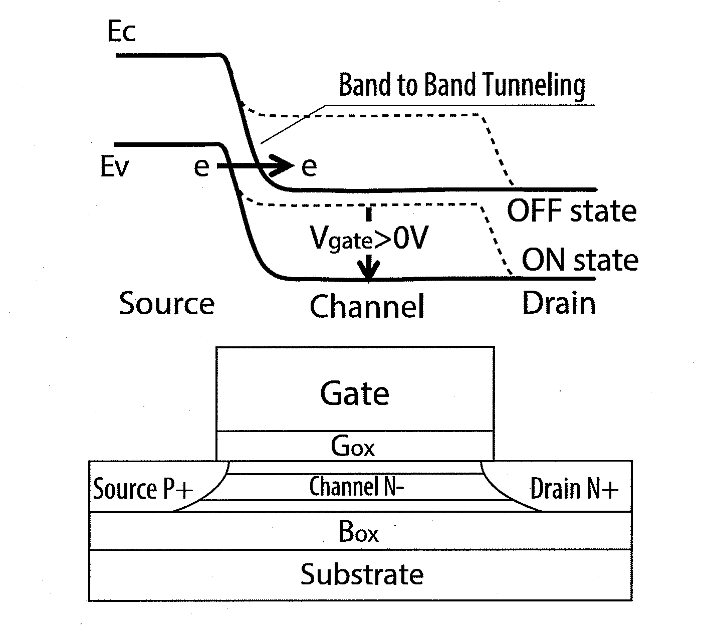
[0066]First, an embodiment of a device simulation system and an embodiment of a device simulation method according to the present invention will be described with reference to drawings. A tunnel-FET (TFET) utilizes a band-to-band tunneling phenomenon that occurs in a source-gate overlap region of the tunnel-FET, for switching on / off of the tunnel-FET. FIG. 1 is a schematic diagram of an N-type TFET. Different from a common CMOS, the tunnel FET has in its source a P+ layer. As shown in an energy band diagram, when the band position of the channel of the N-type TFET is lowered by a gate voltage, a valence band (Ev) and a conduction band (Ec) become closer at an end of the source. Band-to-band tunneling therefore occurs. According to the tunnel-FET, a quick switching characteristic can be obtained due to this principle, compared with a conventional MOS FET. As result, an LSI with the tunnel-FET can be obtained, having a lower power consumption than the CMOS LSI....


PUM


Abstract

A tunnel path of the tunnel FET at a source-gate overlap portion is divided into a vertical path vertical to the source-gate overlap portion and a horizontal path extending to a drain in a horizontal direction along a channel interface. A tunnel distance computation section obtains a tunnel distance for each position of a nonlocal electric field band-to-band tunnel, using first and second bends of the mid-gap potential, which are previously stored approximate functions of the mid-gap potential on the vertical and horizontal paths, respectively. A carrier generation rate computation section computes a carrier generation rate due to band-to-band tunneling, based on the tunnel distance at each position of the nonlocal electric field band-to-band tunnel and a band gap.

Description

FIELD OF THE INVENTION[0001]The present invention relates to device simulation method and device simulation system for a tunnel FET, and compact model design method and compact model for the tunnel FET.BACKGROUND OF THE INVENTION[0002]A tunnel-FET (TFET) has drawn attraction as a key device for implementing a circuit with lower power consumption than with a CMOS. JP2012-182368A (Patent Document 1) discloses a configuration example of the tunnel-FET. JP2009-302419A (Patent Document 2) discloses simulation method and apparatus for a MOSFET.SUMMARY OF THE INVENTION[0003]In device design of a tunnel-FET, a design tool that takes into account of the structure of the tunnel-FET and the influence of material parameters of the tunnel-FET is needed. In circuit design, however, it is a challenge to assemble a circuit using the tunnel-FET that performs an operation completely different from that of a conventional device. A compact model is therefore needed in order to study the circuit design....

Claims


Application Information

Patent Timeline
IPC IPC(8): G06F17/50
CPCG06F17/5009G06F30/367
Inventor FUKUDA, KOICHI
Owner NAT INST OF ADVANCED IND SCI & TECH
Why Eureka
Try Eureka