Reflective Optical Element for the EUV Wavelength Range, Method for Producing and for Correcting Such an Element, Projection Lens for Microlithography Comprising Such an Element, and Projection Exposure Apparatus for Microlithography Comprising Such a Projection Lens

a technology of reflective optical elements and wavelength ranges, which is applied in the direction of photomechanical devices, lighting and heating devices, instruments, etc., can solve the problems of non-uniform and delimited ageing, not taking into account the long-term densification or ageing of substrate materials,

Inactive Publication Date: 2014-10-16
CARL ZEISS SMT GMBH
View PDF3 Cites 5 Cited by
  • Summary
  • Abstract
  • Description
  • Claims
  • Application Information

AI Technical Summary

Benefits of technology

[0008]Therefore, it is an object of the invention to provide a reflective optical element for the EUV wavelength range, a method for producing said reflective optical element, and a meth...

Problems solved by technology

What is disadvantageous about all of the methods mentioned, however, is that they do not take account of the long-term densification or ageing of the substrate material of the order of magnitude of a few % by volume on account of EUV radiation.
Consequently, an optical element corrected by t...

Method used


Image

  • Reflective Optical Element for the EUV Wavelength Range, Method for Producing and for Correcting Such an Element, Projection Lens for Microlithography Comprising Such an Element, and Projection Exposure Apparatus for Microlithography Comprising Such a Projection Lens
  • Reflective Optical Element for the EUV Wavelength Range, Method for Producing and for Correcting Such an Element, Projection Lens for Microlithography Comprising Such an Element, and Projection Exposure Apparatus for Microlithography Comprising Such a Projection Lens
  • Reflective Optical Element for the EUV Wavelength Range, Method for Producing and for Correcting Such an Element, Projection Lens for Microlithography Comprising Such an Element, and Projection Exposure Apparatus for Microlithography Comprising Such a Projection Lens

Examples


Embodiment Construction

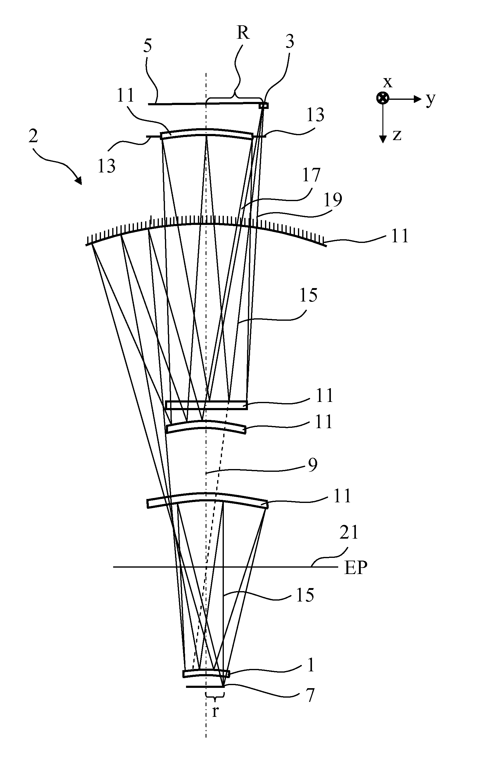
[0031]FIG. 1 shows a schematic illustration of a projection lens 2 according to the invention for a projection exposure apparatus for microlithography composing six mirrors 1, 11, including at least one mirror 1 as optical element according to the invention. The task of a projection exposure apparatus for microlithography is to image the structures of a mask, which is also designated as a reticle, lithographically onto a so-called wafer in an image plane. For this purpose, a projection lens 2 according to the invention in FIG. 1 images an object field 3, which is arranged in the object plane 5, into an image field in the image plane 7. The structure-bearing mask or mask according to the invention, which is not illustrated in the drawing for the sake of clarity, can be arranged at the location of the object field 3 in the object plane 5. For orientation purposes, FIG. 1 illustrates a cartesian coordinate system, the x-axis of which points into the plane of the figure. In this case, t...


PUM

PropertyMeasurementUnit
Lengthaaaaaaaaaa
Lengthaaaaaaaaaa
Lengthaaaaaaaaaa

Abstract

A reflective optical element 39 for EUV wavelengths having a layer arrangement on the surface of a substrate, wherein the layer arrangement includes at least one layer subsystem 37 consisting of a periodic sequence of at least one period of individual layers. The period includes two individual layers having different refractive indices in the EUV wavelength range. The substrate has a variation of the density of more than 1% by volume at least along an imaginary surface 30 at a fixed distance of between 0 μm and 100 μm from the surface. Also, the substrate is protected against long-term aging or densification by EUV radiation either with a protective layer, with a protective layer subsystem of the layer arrangement, or with a correspondingly densified surface region 35 of the substrate.

Description

CROSS-REFERENCE TO RELATED APPLICATIONS[0001]This application is a Continuation Application of International Application No. PCT / EP2012 / 065838, filed on Aug. 14, 2012, which claims benefit under 35 U.S.C 119(e) of U.S. Provisional Application No. 61 / 544,361, filed Oct. 7, 2011, and which claims priority under 35 U.S.C. §119(a) to German Patent Application No. 10 2011 084 117.2, filed Oct. 7, 2011. The entire disclosures of all three related applications are considered part of and are incorporated by reference into the disclosure of the present application.FIELD OF AND BACKGROUND OF THE INVENTION[0002]The invention relates to a reflective optical element for the EUV wavelength range. Furthermore, the invention relates to a method for producing and to a method for correcting such an element. Furthermore, the invention relates to a projection lens for microlithography comprising such an element and to a projection exposure apparatus for microlithography comprising such a projection len...

Claims


Application Information

Patent Timeline
IPC IPC(8): G02B5/08B29D11/00G02B13/14
CPCG02B5/0891B29D11/00865B29D11/00009G02B13/143G03F7/70591G03F7/70958G21K1/062G21K2201/067G03F7/70316G03F1/24G03F1/60G03F1/72B82Y10/00
Inventor WEISS, MARKUSKERWIEN, NORBERTWEISER, MARTINBITTNER, BORISWABRA, NORBERTSCHLICHENMAIER, CHRISTOPHCLAUSS, WILFRIED
Owner CARL ZEISS SMT GMBH
Why Eureka
Try Eureka