Electro-optical device and electronic apparatus

a manufacturing method and electrooptical technology, applied in non-linear optics, instruments, optics, etc., can solve the problems of inability to generate cracks due to thermal stress in the gate electrode and the periphery, and the risk of wiring being cut, etc., to achieve stable device operation, excellent cost performance, and high manufacturing yield

Active Publication Date: 2014-10-23
138 EAST LCD ADVANCEMENTS LTD
View PDF1 Cites 13 Cited by
  • Summary
  • Abstract
  • Description
  • Claims
  • Application Information

AI Technical Summary

Benefits of technology

[0033]According to these application examples, there is included the electro-optical device that has the gate wiring unlikely to be cut to ensure a stable device operation even if the stress is concentrated between the peripheral circuit region and the dummy pixel region, and that can be manufactured at a high manufacturing yield. Accordingly, it is possible to provide electronic apparatuses with excellent cost performance.

Problems solved by technology

In particular, in the case where part of the dummy pixel shielding film is used as wiring, there is a risk that the wiring is cut due to the crack.
According to this method, since the gate electrodes are formed using a conductive poly-silicon film having a lower coefficient of thermal expansion than metal such as aluminum, cracks due to the thermal stress are unlikely to be generated in the gate electrodes and the periphery thereof.

Method used


Image

  • Electro-optical device and electronic apparatus
  • Electro-optical device and electronic apparatus
  • Electro-optical device and electronic apparatus

Examples


first embodiment

[0047]In a first embodiment, an active-matrix liquid crystal device equipped with thin-film transistors serving as switching elements of pixels will be cited and described as an example of an electro-optical device. This liquid crystal device is a device that can be favorably used as a light modulation unit (liquid crystal light valve) of a projection display apparatus (liquid crystal projector) to be explained later, for example.

Liquid Crystal Device

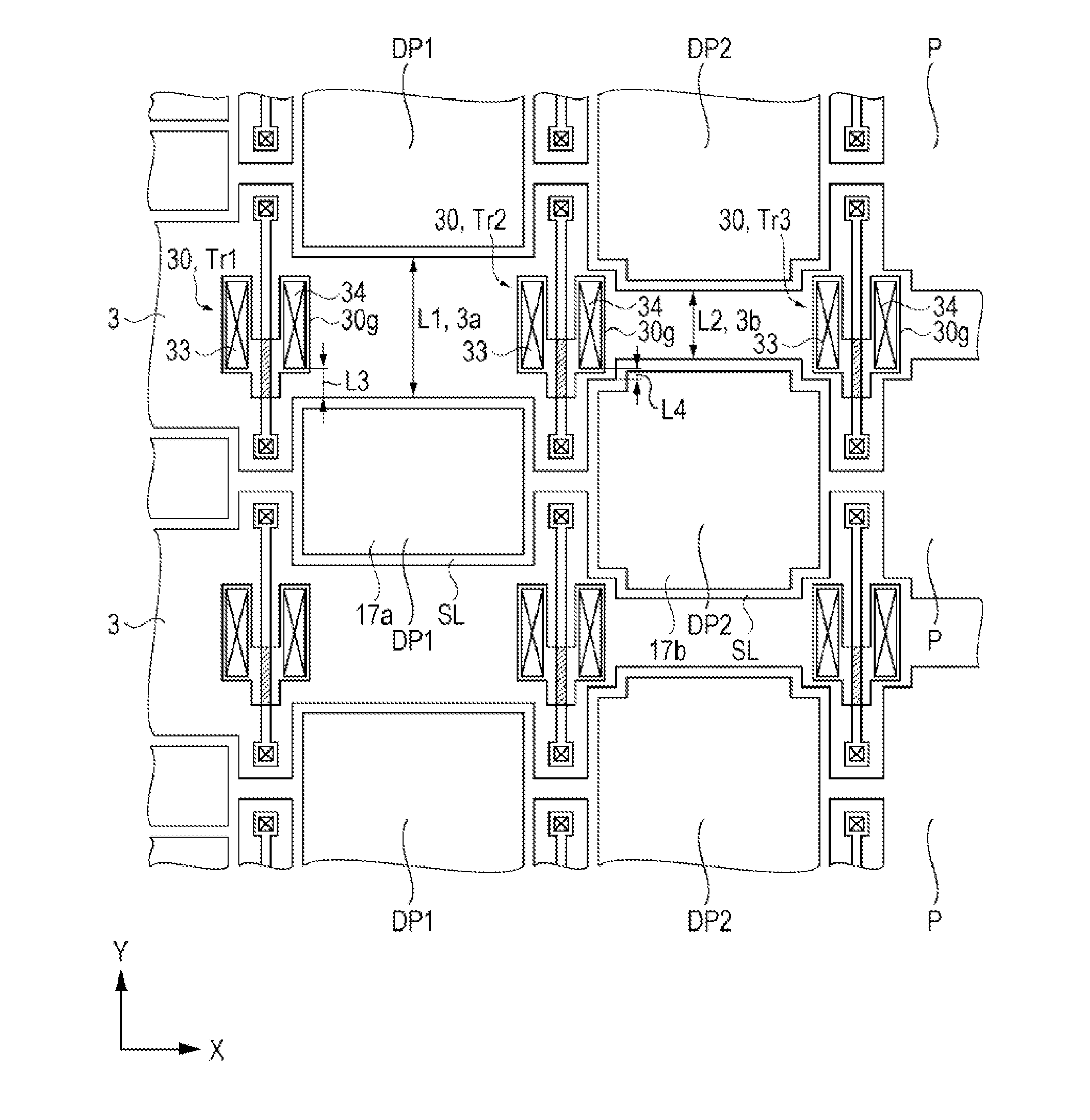
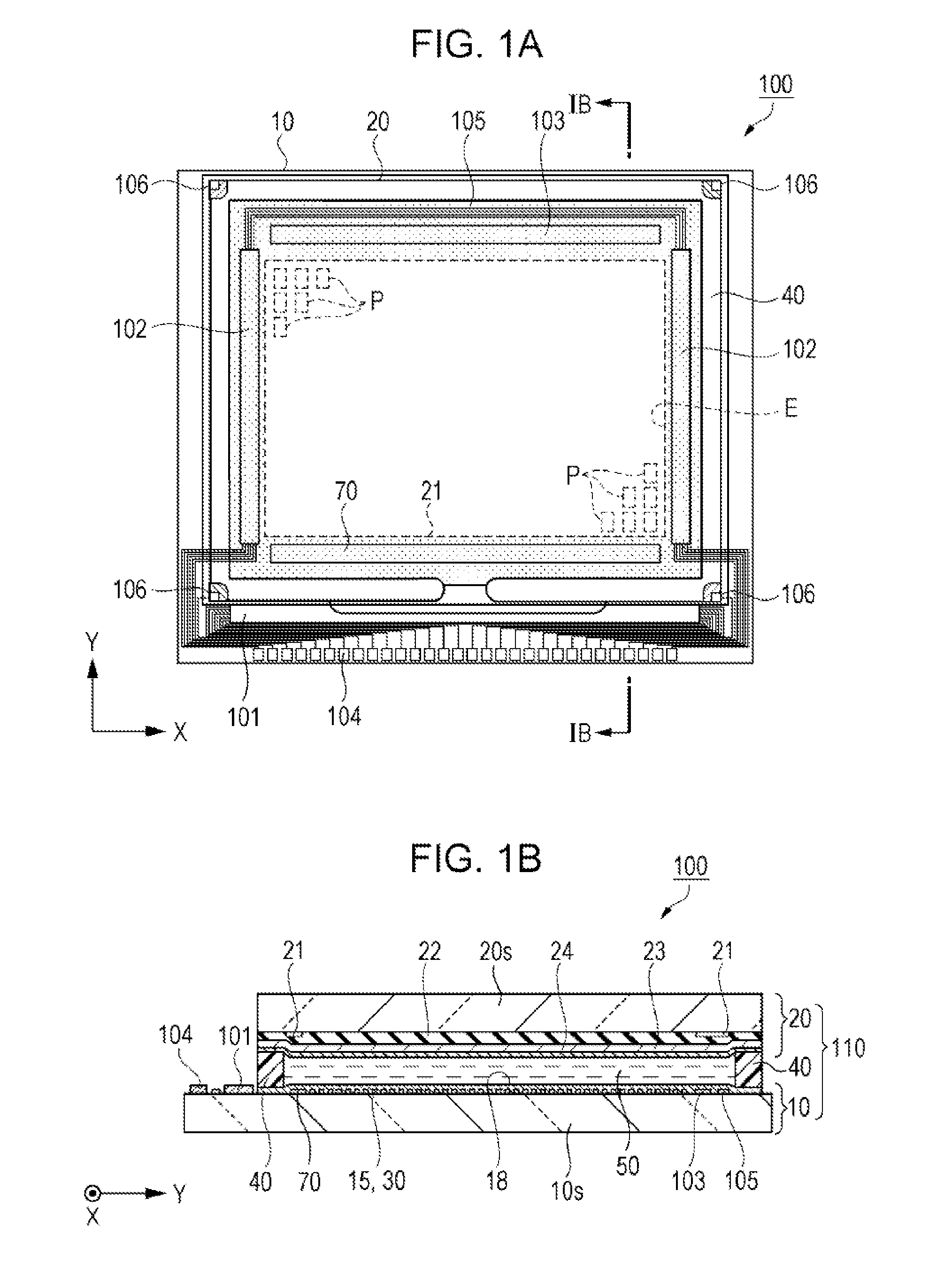
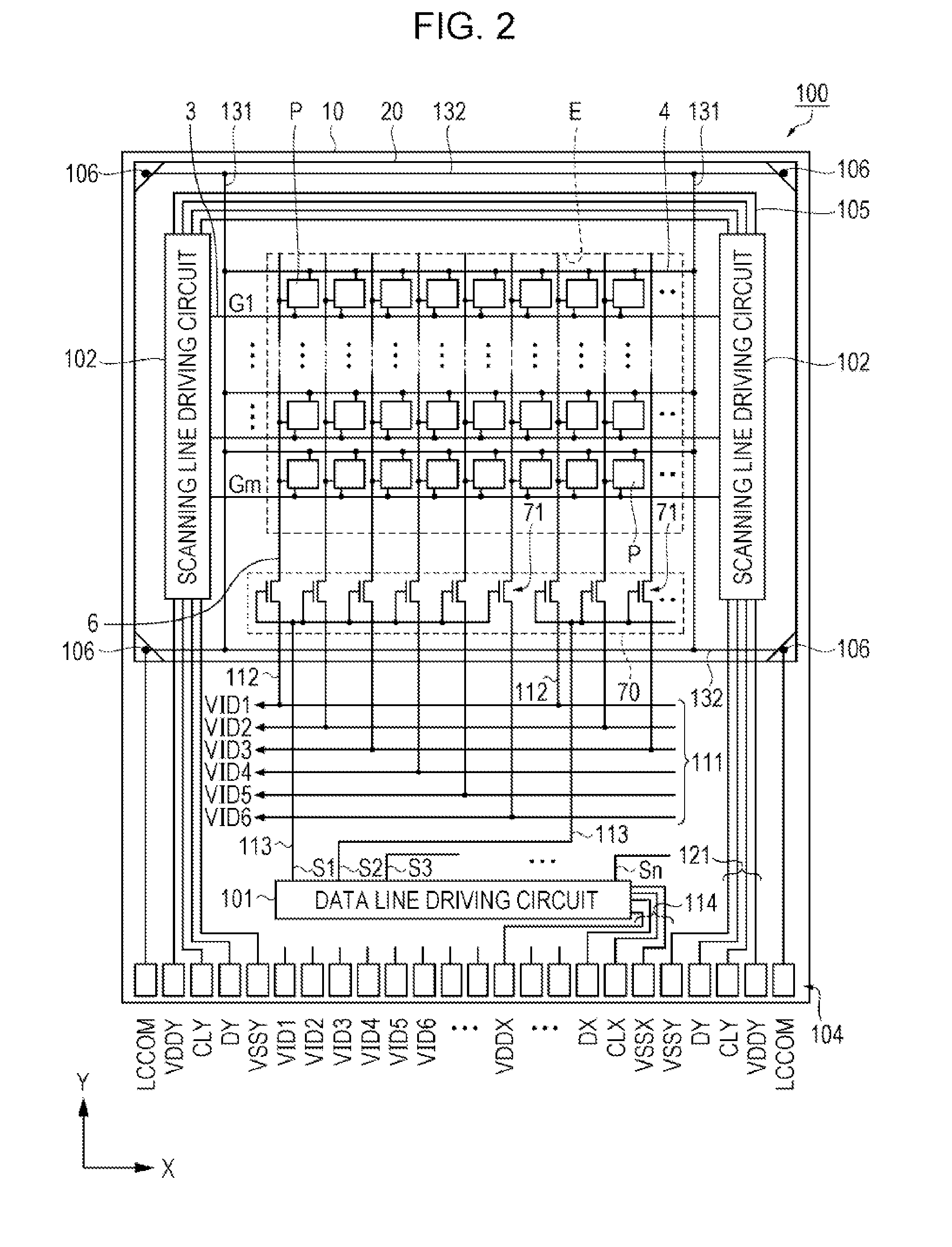
[0048]First, the overview of a liquid crystal device as an electro-optical device of this embodiment will be described with reference to FIG. 1A through FIG. 3. FIG. 1A is a schematic plan view illustrating a configuration of the liquid crystal device, FIG. 1B is a schematic cross-sectional view illustrating a structure of the liquid crystal device taken along a line IB-IB in FIG. 1A. FIG. 2 is a circuit diagram illustrating an electrical configuration of the liquid crystal device, and FIG. 3 is an equivalent circuit diagram illustratin...

second embodiment

[0137]Electronic Apparatus

[0138]Next, a projection display apparatus as an electronic apparatus will be described with reference to FIG. 10. FIG. 10 is a schematic diagram illustrating a configuration of a projection display apparatus.

[0139]As shown in FIG. 10, a projection display apparatus 1000 as an electronic apparatus according to a second embodiment of the invention includes: a polarization illumination device 1100 disposed along a system optical axis L; two dichroic mirrors 1104 and 1105 as light separation elements; three reflection mirrors 1106, 1107, and 1108; five relay lenses 1201, 1202, 1203, 1204, and 1205; three transmissive liquid crystal light valves 1210, 1220, and 1230 as light modulation units; a cross dichroic prism 1206 as a light combination element; and a projection lens 1207.

[0140]The polarization illumination device 1100 is generally configured of a lamp unit 1101 as a light source formed with a white light source such as an ultrahigh pressure mercury lamp ...


PUM

PropertyMeasurementUnit
widthaaaaaaaaaa
lengthaaaaaaaaaa
thicknessaaaaaaaaaa

Abstract

A liquid crystal device includes a first dummy pixel and a second dummy pixel adjacent to each other in an X direction, in which width of a first portion of a scanning line between a first transistor of the first dummy pixel and a second transistor of the second dummy pixel is larger than width of a second portion of the scanning line between the second transistor and a third transistor of a pixel.

Description

BACKGROUND[0001]1. Technical Field[0002]The present invention relates to electro-optical devices, manufacturing methods for electro-optical devices, and electronic apparatuses.[0003]2. Related Art[0004]As an electro-optical device, such an electro-optical device is disclosed (Japanese Patent No. 4,798,186) that includes, on a substrate, an image display region where a plurality of pixels are arranged, a dummy region located in the circumference of the image display region where a plurality of dummy pixels are arranged, and a dummy pixel shielding film provided in the dummy region across the plurality of dummy pixels; further, in the disclosed electro-optical device, slits are provided in the dummy pixel shielding film for each of the dummy pixels.[0005]According to the electro-optical device described in Japanese Patent No. 4,798,186, by providing the dummy pixel shielding film corresponding to opening regions of the dummy pixels, oblique light that enters the dummy region in an obl...

Claims


Application Information

Patent Timeline
Patent Type & Authority Applications(United States)
IPC IPC(8): G02F1/1362G02F1/1368
CPCG02F1/136209G02F1/136286G02F1/1368G02F1/133509G02F1/136277G02F1/133388
Inventor KINOE, YUSUKE
Owner 138 EAST LCD ADVANCEMENTS LTD
Why Eureka
Try Eureka