Semiconductor device and method for manufacturing such a semiconductor device

a semiconductor and semiconductor technology, applied in the field of power electronics, can solve problems such as premature breakdown of devices, and achieve the effects of reliable manufacturing method, improved device operation, and high quality

Active Publication Date: 2018-10-04
HITACHI ENERGY SWITZERLAND AG
View PDF0 Cites 4 Cited by
  • Summary
  • Abstract
  • Description
  • Claims
  • Application Information

AI Technical Summary

Benefits of technology

[0017]The masks for forming the well and the channel layers are self-aligned to the mask for forming the n source regions, which makes the manufacturing method reliable and of high quality due to the mask for forming the plug covering the n source regions completely, there is no overcompensation of the charges of the n source regions and the plug, which means that there is no neutral zone in the device, which allows better operation of the device. The channel and well layers have a much lower doping concentration than the source regions, so that an overcompensation of these layers does not lead to a neutralized zone, but allows to provide an easy manufacturing method.
[0018]A MOS (metal-oxide-semiconductor) cell is formed by the layers / regions mentioned beforehand. The deep highly doped plug improves the contact to the well layer. Its depth is as least as great as the depth of the well layer to protect the channel layers of the MOS cell from peaks of the electric field, which are highest underneath the center of the MOS cell, i.e. below the location of the plug. This avoids undesired parasitic actions (parasitic transistor in case of a MOSFET and parasitic thyristor in case of an IGBT) as well as it diminishes short-channel effects (see FIG. 19). In this FIG. 19, it is shown that for a 300 nm wide channel (being the extension of the channel layer between the source region and the drift layer) the leakage current abruptly rises for forward blocking voltages smaller than the avalanche breakdown voltage, resulting in a premature breakdown of the device. For an inventive MOSFET with the same channel width, breakdown can be shifted to higher forward blocking voltages.
[0019]In addition the strength of the electric field in the gate-insulator gets reduced by the plug, wherein the effect is more pronounced for deeper plugs. The FIGS. 15 to 18 show the electric fields through different planes of the MOS-cell of the device. In FIGS. 15 to 18, the plug depth is given relative to the depth of the p well layer. “Prior Art” means that the plug is less deep than the p-well layer. “D1” means that the plug and the p-well layer have the same depth. “D2” shall mean that the plug depth is 1.5 times the well layer depth and “D3” means that the plug depth is two times larger than the well layer depth.
[0020]FIG. 15 shows the electric field from the first to the second main side between two MOS cells (cut along line A-A in FIG. 2). FIG. 16 is a detail from FIG. 15 at the interface between the first insulating layer 72 of the gate electrode 7 and the drift layer 2 (dotted area of FIG. 15). From this figure it is obvious, that the electric field is reduced in the wide bandgap material as well as in the insulating layer of the gate electrode (e.g. gate oxide). FIG. 17 shows the electric field in a plane parallel to the first main side (cut along line B-B in FIG. 2); showing the electric field in a non-depleted region 47 of the channel layer and in a depleted region 48 of the channel layer. FIG. 18 shows the electric field along line C-C in FIG. 2, which plane lies parallel to line A-A and goes through the channel layer. For all planes, a tremendous reduction of the electric field is obvious, this effect even being larger, because of the plug in the prior art devices having a plug depth, which is smaller as compared to the well layer depth.

Problems solved by technology

In this FIG. 19, it is shown that for a 300 nm wide channel (being the extension of the channel layer between the source region and the drift layer) the leakage current abruptly rises for forward blocking voltages smaller than the avalanche breakdown voltage, resulting in a premature breakdown of the device.

Method used


Image

  • Semiconductor device and method for manufacturing such a semiconductor device
  • Semiconductor device and method for manufacturing such a semiconductor device
  • Semiconductor device and method for manufacturing such a semiconductor device

Examples


Embodiment Construction

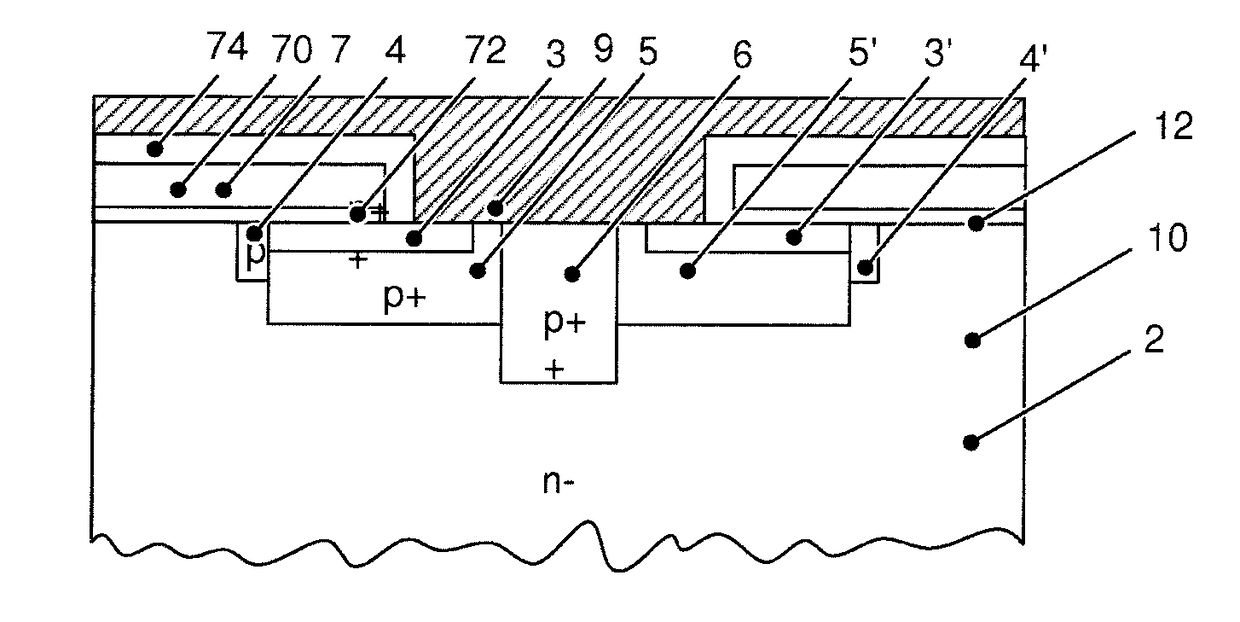
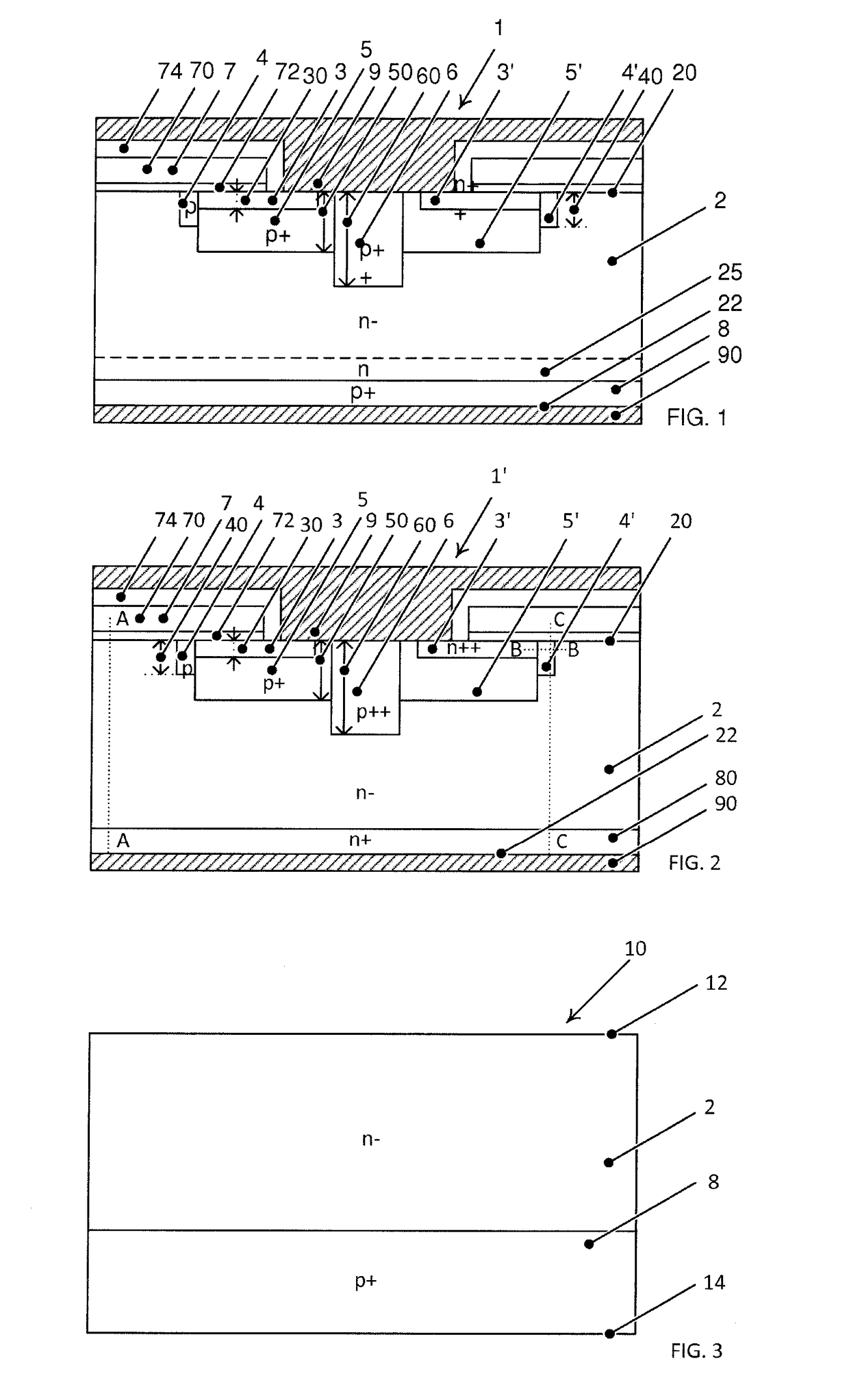
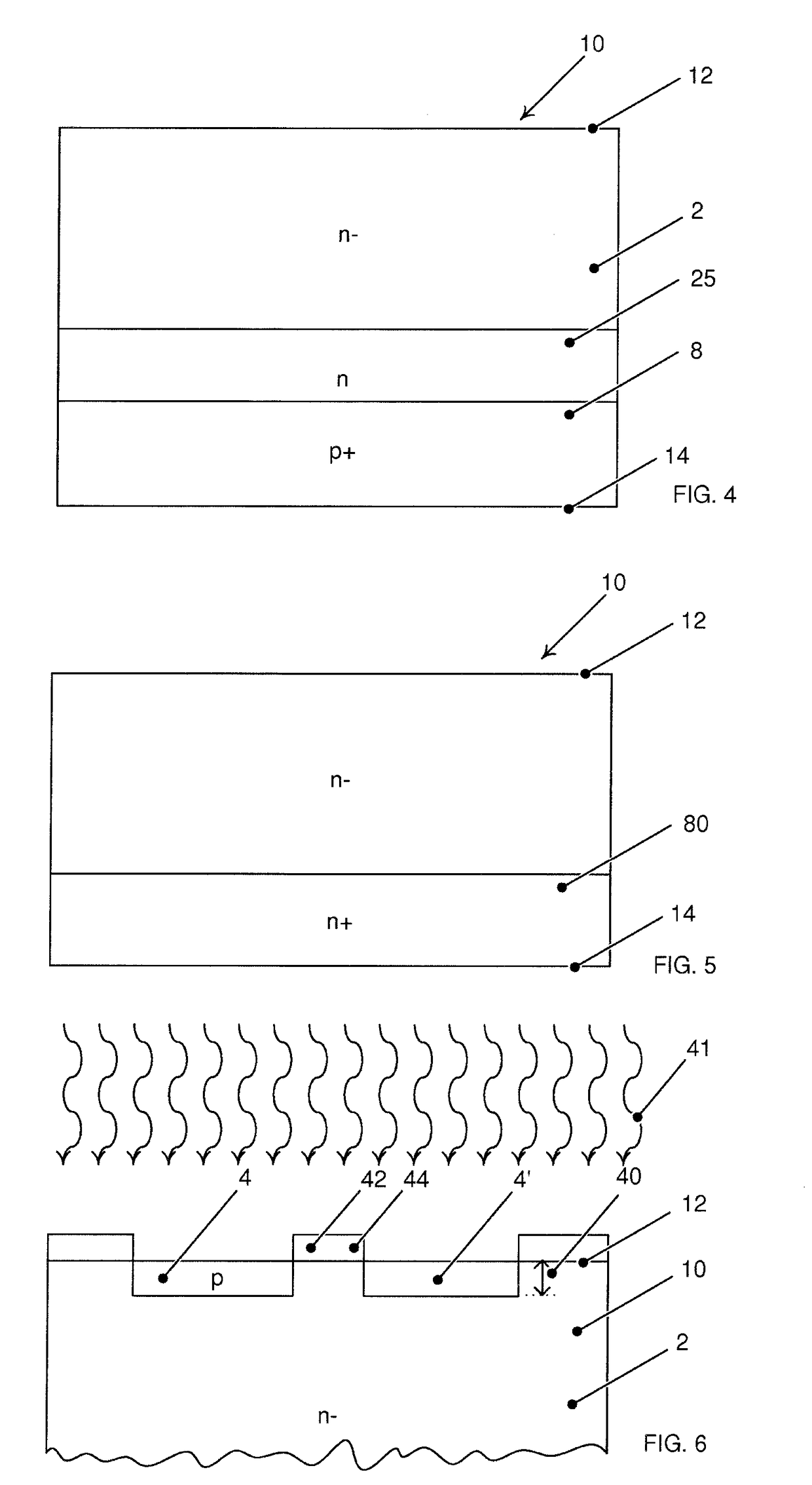
[0033]FIG. 1 shows an inventive insulated gate bipolar transistor (IGBT) 1. The IGBT 1 is a wide bandgap device, e.g. a silicon carbide device, comprising a lowly (n−) doped drift layer 2 between a first main side 20 and a second main side 22 of the device opposite to the first main side 20. Wide band gap materials shall be materials having a bandgap of at least 2 eV like silicon carbide, gallium nitride or diamond not excluding other wide bandgap materials. Depending on the voltage class, the doping concentration and thickness of the drift layer 2 are chosen. Exemplarily, the drift layer 2 has a doping concentration between 1*1012 and 1*1017 cm−3 and a thickness between 1 to 500 μm. The thicknesses shall be measured in depth direction, i.e. in a direction vertical to the first main side 20.

[0034]For an inventive IGBT, a p+ doped collector layer 8 is arranged on the second main side 22 and has exemplarily a doping concentration between 1*1018 and 1*1020 cm−3. The collector layer 8 c...


PUM


Abstract

A method of manufacturing a semiconductor device is provided with: (a) providing a wide bandgap substrate product, (b) for forming two channel layers applying a first mask and applying a p first dopant, for forming two source regions forming a second mask by applying a further layer on the lateral sides of the first mask and applying an n second dopant, for forming two well layers forming a third mask by removing such part of the second mask between the source regions and applying a p third dopant, wherein a well layer depth is at least as large as a channel layer depth, (c) after step (b) for forming a plug applying a fourth mask, which covers the source regions and the channel layers and applying a p fourth dopant to a greater depth than the well layer depth and with a higher doping concentration than the well layers; wherein the well layers surround the plug in the lateral direction and separate it from the two source regions.

Description

TECHNICAL FIELD[0001]The invention relates to the field of power electronics and more particularly to a method for manufacturing a semiconductor device and to such a semiconductor device.BACKGROUND ART[0002]In FIG. 14 a prior art MOSFET 100 is shown as known from U.S. Pat. No. 7,074,643 B2. The prior art MOSFET 100 is made of an n+ silicon carbide (SiC) substrate 80 and comprises between a first main side 20 and a second main side 22 an n− doped drift layer 2. On the first main side 20, two n++ doped source regions 3, 3′ are arranged, each which is separated from the drift layer 2 in lateral direction (i.e. in a direction parallel to the first main side 20) by a p doped channel layer 4, 4′ and on a side opposite to the first main side 20 by a p+ well layer 5, 5′, which is higher doped than the channel layer 4, 4′. In between such two source regions 3, 3′ surrounded by a channel layer 4, 4′ and a well layer 5, 5′, a p++ doped contact layer 65 is arranged, which laterally extends to t...

Claims


Application Information

Patent Timeline
Patent Type & Authority Applications(United States)
IPC IPC(8): H01L29/66H01L29/10H01L29/08H01L21/04H01L29/36H01L29/06H01L29/16H01L29/78H01L29/739
CPCH01L29/36H01L29/0696H01L29/1608H01L29/0634H01L29/0821H01L29/7811H01L29/7395H01L29/66333H01L29/66712H01L29/66068H01L29/1095H01L29/0865H01L29/086H01L29/1033H01L21/0465H01L21/049H01L21/0485H01L29/7802H01L29/2003H01L21/266
Inventor BARTOLF, HOLGERRAHIMO, MUNAFKNOLL, LARSMIHAILA, ANDREIMINAMISAWA, RENATO
Owner HITACHI ENERGY SWITZERLAND AG
Why Eureka
Try Eureka