Eureka AIR delivers breakthrough ideas for toughest innovation challenges, trusted by R&D personnel around the world.

Semiconductor structure with sacrificial anode and method for forming

Active Publication Date: 2014-11-27
NXP USA INC
View PDF2 Cites 15 Cited by
  • Summary
  • Abstract
  • Description
  • Claims
  • Application Information

AI Technical Summary

Benefits of technology

The present invention relates to a semiconductor structure with a sacrificial anode for preventing corrosion in wire bond technology. The technical effect of the invention is to improve the reliability of wire bonding by attracting corrosive species to the sacrificial anode instead of the important intermetallic compound of the wire bond, resulting in better performance of the semiconductor structure. The invention includes a method for forming a sacrificial layer over a conductive layer and a patterned masking layer, followed by etching and removal of the sacrificial layer and conductive layer to create a bond pad. The use of a sacrificial anode in wire bond technology has been previously limited due to the difficulty in preventing corrosion in the intermetallic compound of the wire bond. The invention provides a solution for improving the reliability of wire bonding in semiconductor structures.

Problems solved by technology

This corrosion results in open failures of the wire bonds, such as during temperature / humidity reliability testing.

Method used


Image

  • Semiconductor structure with sacrificial anode and method for forming
  • Semiconductor structure with sacrificial anode and method for forming
  • Semiconductor structure with sacrificial anode and method for forming

Examples


Embodiment Construction

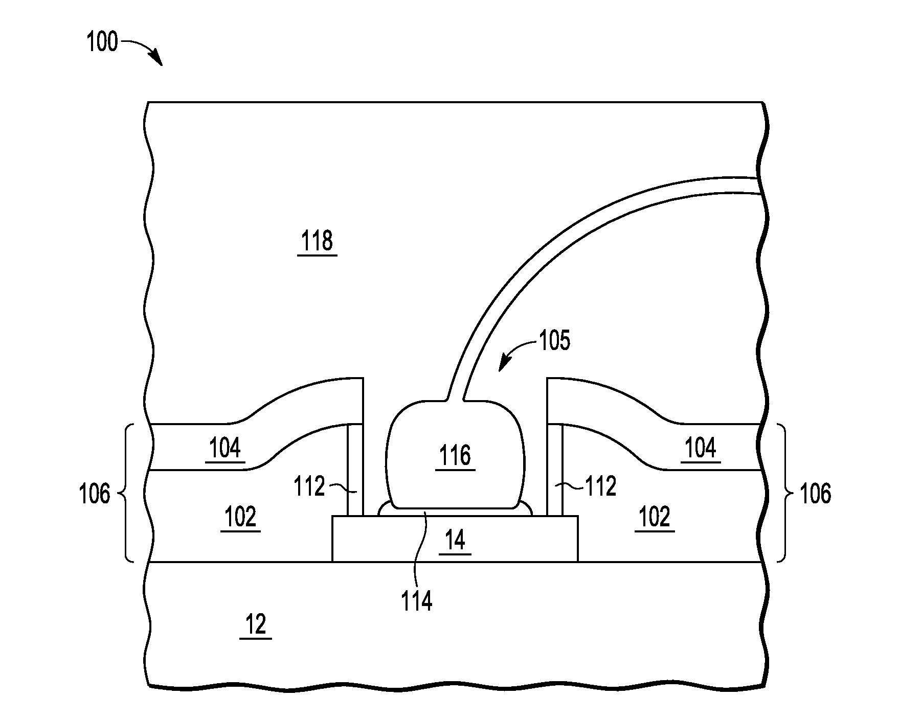
[0009]In order to prevent corrosive species from attacking the wire bond IMC, a sacrificial anode is formed in order to attract the corrosive species. In this manner, the sacrificial anode is corroded instead of the IMC, thus resulting in improved reliability of the wire bond.

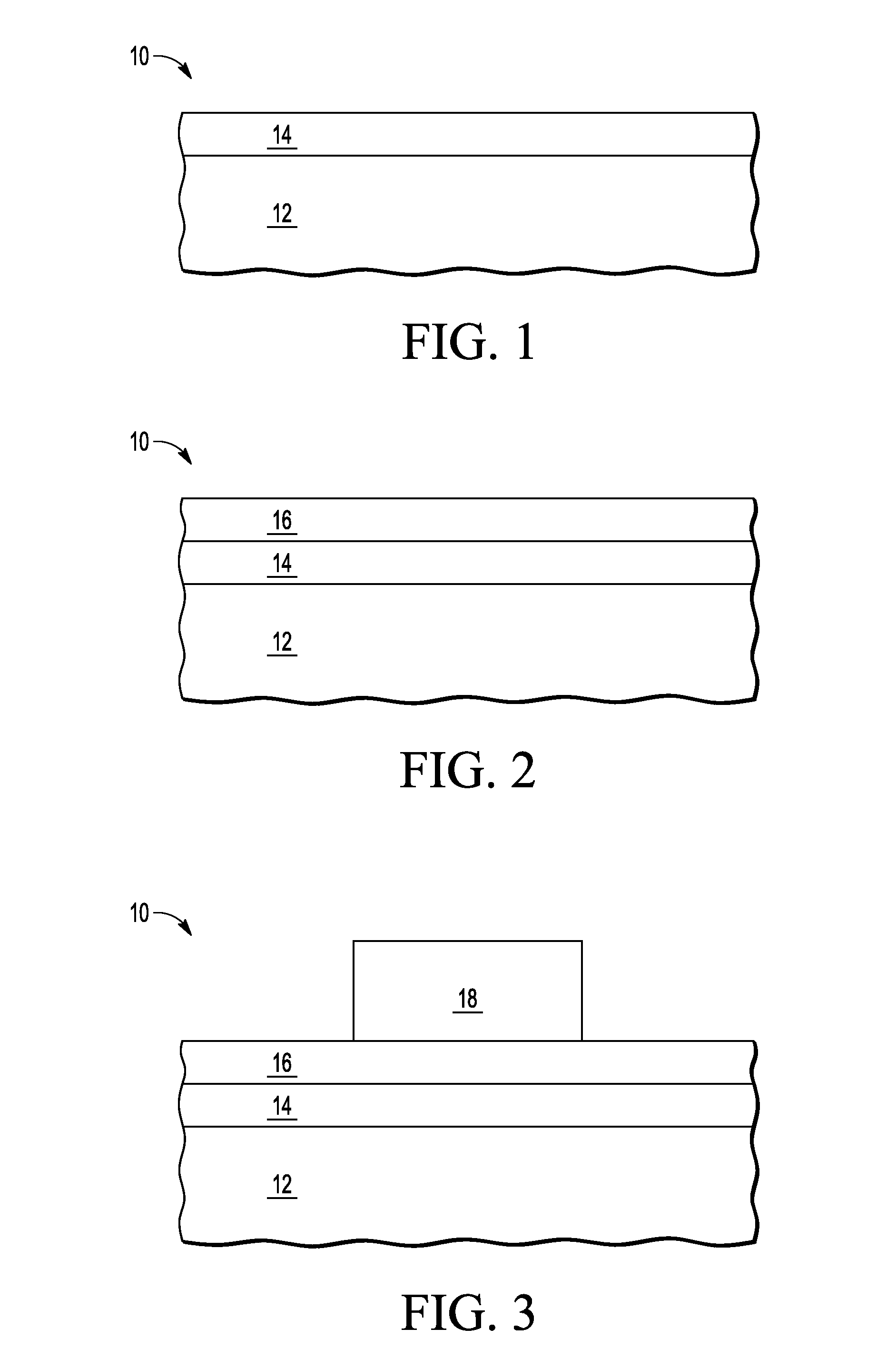
[0010]FIG. 1 illustrates, in cross sectional form, a portion of a semiconductor structure 10 having a semiconductor wafer 12 and a conductive layer 14 formed over wafer 12. Wafer 12 may include any type of semiconductor substrate with active circuitry formed in and on the semiconductor substrate. Wafer 12 also includes any number of interconnect layers formed over the structure which may provide connections between the active circuitry and bond pads which may be formed from conductive layer 14. In one embodiment, conductive layer 14 is blanket deposited over wafer 12 and includes a metal, such as aluminum. Conductive layer 14 will be used to form bond pads on a top surface of wafer 12.

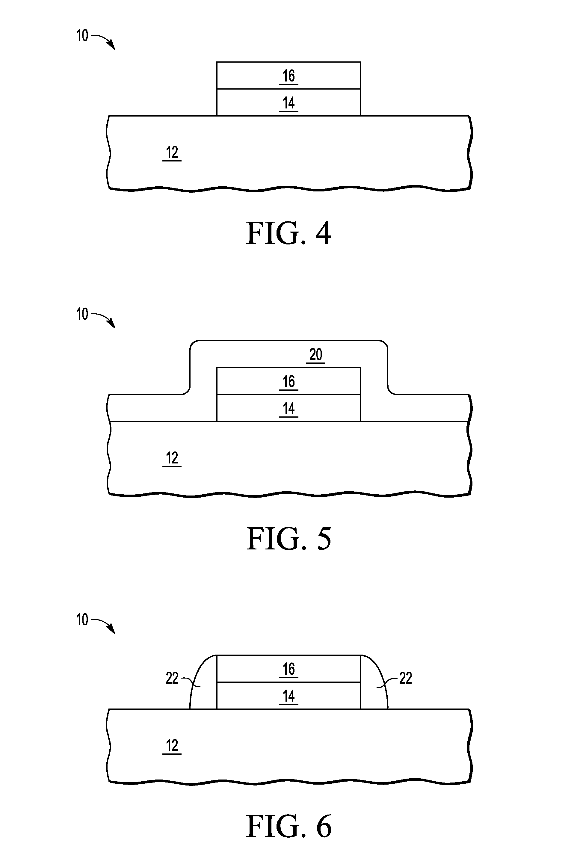
[0011]FIG. 2 illustrates, ...


PUM


Abstract

A packaged semiconductor device is made by forming a conductive pad on an external surface of an integrated circuit device, forming a passivation layer over the conductive pad, removing a portion of the passivation layer over a bond area on the conductive pad, forming a sacrificial anode around a majority of a periphery surrounding the bond area, forming a conductive bond in the bond area, and forming an encapsulating material around the conductive bond and an exposed portion of the sacrificial anode.

Description

BACKGROUND[0001]1. Field[0002]This disclosure relates generally to semiconductor processing, and more specifically, to a semiconductor structure with sacrificial anode.[0003]2. Related Art[0004]With copper wire bond technology, corrosive species from surrounding materials, such as the encapsulant, die attach epoxy, and substrate migrate under moisture, temperature, and voltage environments to the intermetallic compound (IMC) of the wire bond causing corrosion. This corrosion results in open failures of the wire bonds, such as during temperature / humidity reliability testing.BRIEF DESCRIPTION OF THE DRAWINGS[0005]The present invention is illustrated by way of example and is not limited by the accompanying figures, in which like references indicate similar elements. Elements in the figures are illustrated for simplicity and clarity and have not necessarily been drawn to scale.[0006]FIGS. 1-11 illustrate cross sectional views of a semiconductor structure at various stages in processing,...

Claims


Application Information

Patent Timeline
IPC IPC(8): H01L23/00
CPCH01L24/11H01L2224/0391H01L2224/022H01L24/13H01L2224/04042H01L2224/0401H01L2224/05H01L2224/131H01L2224/13147H01L2924/014H01L2924/00014H01L2224/03005H01L23/3192H01L24/03H01L24/45H01L2224/034H01L2224/05567H01L2224/05624H01L2224/45147H01L2224/48463H01L2924/10253H01L2924/10271H01L2924/10329H01L2924/14H01L2224/03019H01L2224/03009H01L2224/03015H01L2224/0218H01L2224/48824H01L2224/02166H01L2224/73265H01L24/05H01L2224/48507H01L2924/00H01L2224/32145H01L2224/48227H01L2224/45124H01L2924/01029H01L24/02H01L24/48H01L2224/0219H01L2224/03622H01L2224/05565H01L2924/01012H01L2924/0103H01L2924/365H01L2924/3651
Inventor CHOPIN, SHEILA F.DING, MINMATHEW, VARUGHESEROTH, SCOTT S.
Owner NXP USA INC
Why Eureka
Eureka Blog
Learn More