Method for Producing Group III Nitride Semiconductor and Group III Nitride Semiconductor

Active Publication Date: 2014-12-04
TOYODA GOSEI CO LTD
View PDF2 Cites 5 Cited by
  • Summary
  • Abstract
  • Description
  • Claims
  • Application Information

AI Technical Summary

Benefits of technology

[0038]According to the first aspect, when the Group III nitride semiconductor is vertically grown in the c-axis direction on the top surfaces of the posts and the bottom surfaces of the trenches on the post-formed substrate, the normal vector of the a-plane of the growing Group III nitride semiconductor has a component perpendicular to the first processed side surface and parallel to the main surface. Since the crystal growth is faster in the a-axis direction than in the m-axis direction, the Group III nitride semiconductor is also grown in the direction parallel to the main surface of the substrate. The normal vector of the a-plane of the growing Group III nitride semiconductor has a larger component in a direction perpendicular to the second processed side surface. In the initial growth stage of Group III nitride semiconductor, the growth of triangle facets comprising the inclined m-plane is faster. Therefore, the facets of Group III nitride semiconductor in a stripe pattern parallel to the first direction of first stripe structure are formed. As a result, Group III nitride semiconductor is laterally grown as well as facet grown in the direction perpendicular to the main surface under the vertical growth conditions,

Problems solved by technology

However, when Group III nitride semiconductor is grown on the concave-convex sapphire substrate by these methods, voids are formed near the side surfaces of the trenches or posts, resulting in a problem that crystallinity and flatness of Group III nitride semiconductor are deteriorated.
When the trenches or posts are formed in such a manner, GaN is grown on the top surfaces of the posts of the sapphire substrate and the bottom surfaces of the trenches, and GaN is difficult to grow on side surfaces of the trenches or posts.
On the other hand, when sides in planar view of trenches or posts are parallel to an a-plane of a s

Method used


Image

  • Method for Producing Group III Nitride Semiconductor and Group III Nitride Semiconductor
  • Method for Producing Group III Nitride Semiconductor and Group III Nitride Semiconductor
  • Method for Producing Group III Nitride Semiconductor and Group III Nitride Semiconductor

Examples


embodiment 1

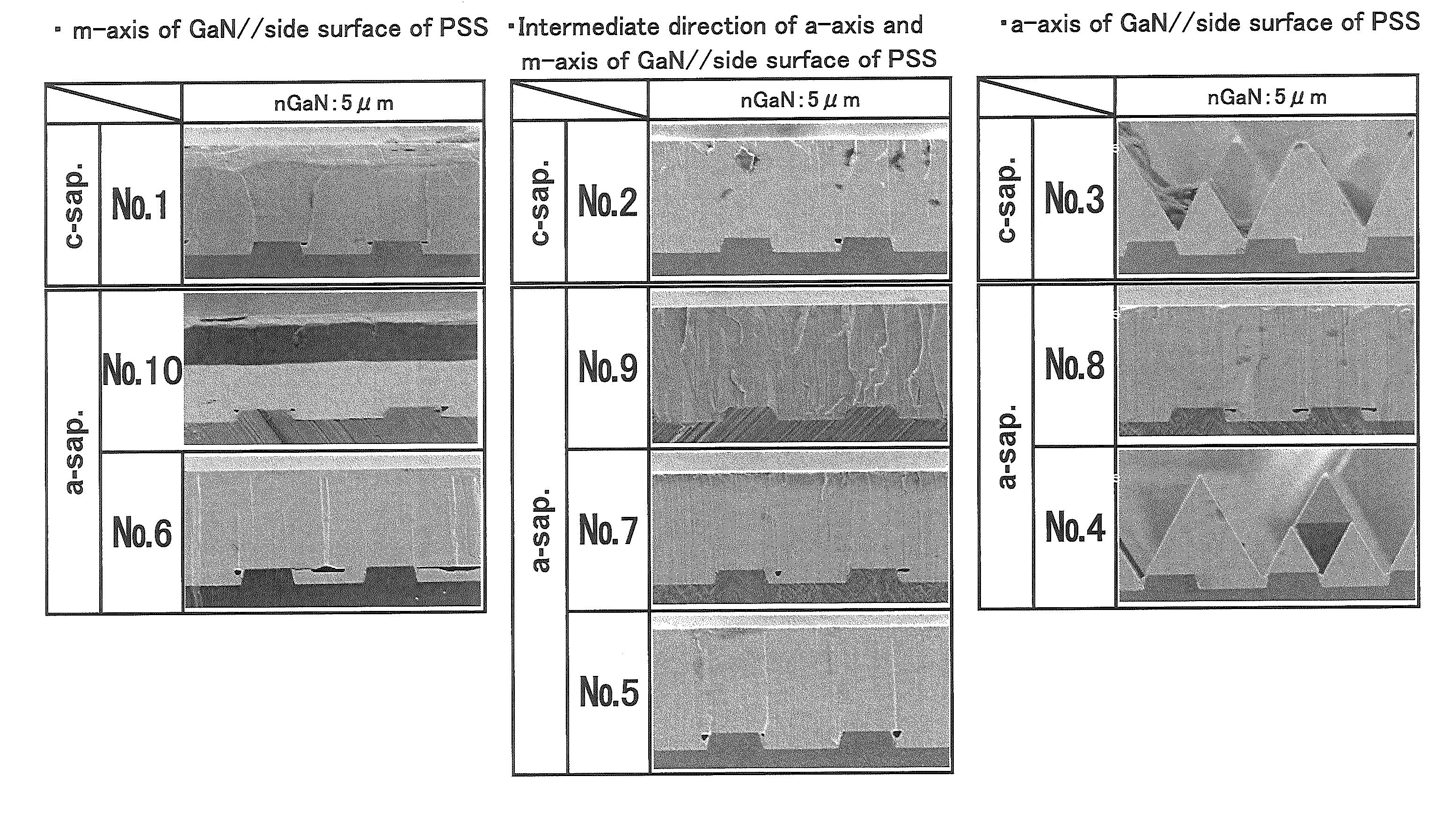
[0068]Firstly, a relationship between the crystal orientation of the stripe structure and the crystal quality of grown GaN will be described.

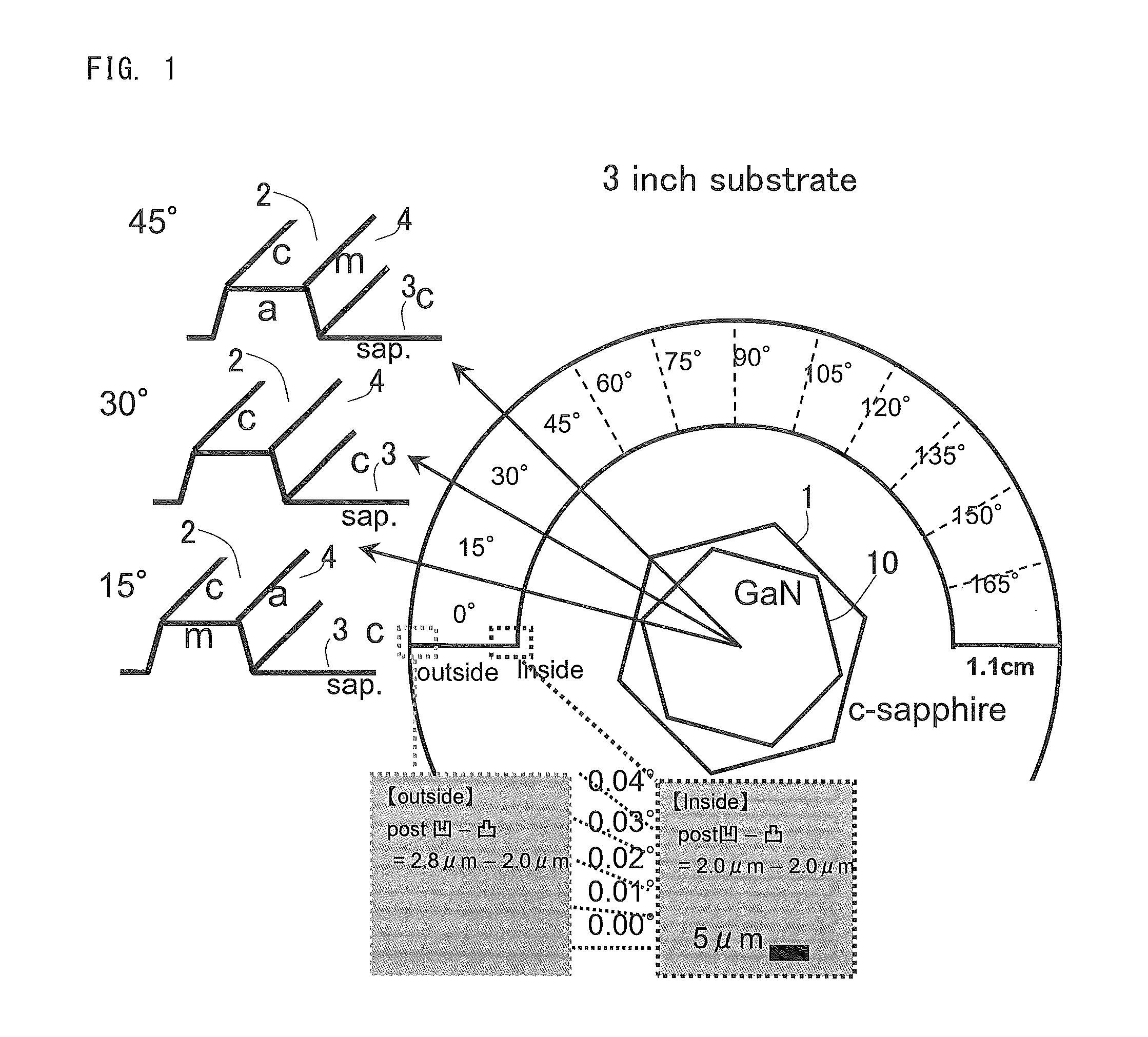
[0069]GaN crystals were grown on a sapphire substrate having a thickness of 500 μm and a c-plane main surface on which processed side surfaces are formed in different crystal orientations. As shown in FIG. 1, posts 2 and trenches 3 were radially formed in a stripe pattern on the main surface of the sapphire substrate. The posts 2 and the trenches 3 were formed by forming the trenches 3 through dry etching. An interval angle of adjacent posts 2 is 0.01°. Each of the trenches 3 has a depth of 0.7 μm. Each of the trenches 3 has a width of 2.0 μm, and each of the posts 2 has a width of 2.0 μm. After the processed substrate was placed in a MOCVD growth apparatus and cleaned with a hydrogen gas, an AlN low-temperature buffer layer was formed. Thereafter, GaN was grown under the conditions for vertical growth.

[0070]In FIG. 1, when a stripe of post 2 i...

embodiment 2

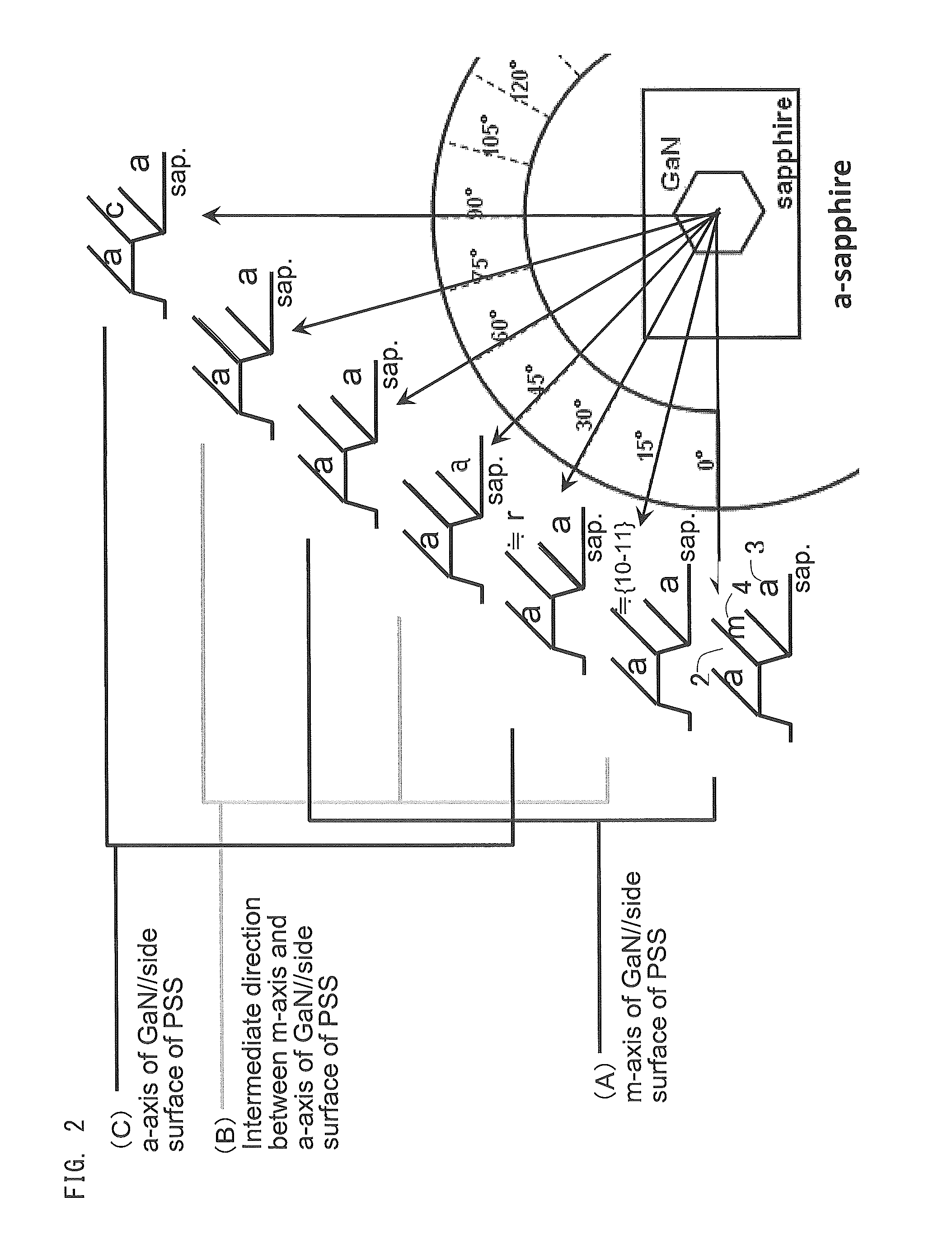
[0102]Next will be described the case where GaN crystals were grown on a sapphire substrate having an a-plane main surface. In the present embodiment as well, the processed side surface is considered as perpendicular to the main surface of the substrate for ease of explanation. As shown in FIG. 2, posts 2 and trenches 3 were radially formed at an interval angle of 0.01° on the main surface of sapphire. In FIG. 2, when the stripe direction of the post 2 is in a direction of 0° to the baseline of the sapphire substrate, the side surface 4 of the post 2 is the m-plane of sapphire (the lateral vector is the m-axis). When the stripe direction of the post 2 is in a direction of 90° to the baseline of the sapphire substrate, the side surface 4 of the post 2 is the c-plane of sapphire (the lateral vector is the c-axis). When the stripe direction is in an intermediate direction of 30° between 0° and 90°, the side surface 4 of the post 2 is a plane close to the r-plane (−1012) of sapphire (th...

embodiment 3

[0111]This embodiment is an example using a Group III nitride semiconductor substrate instead of a sapphire substrate in Embodiments 1 and 2. In this case, as shown in FIG. 21, the main surface of the substrate is a c-plane. A concave-convex structure was formed so that the first angle θ1 between the first lateral vector t of the first processed side surface 100aa of the first stripe structure 100 on the substrate and the m-axis projected vector m obtained by orthogonally projecting the normal vector of the m-plane to the main surface of the substrate is from 0.5° to 6°, and the second angle θ2 between the second lateral vector s of the second processed side surface 101aa of the second stripe structure 101 and the a-axis projected vector a obtained by orthogonally projecting the normal vector of the a-plane to the main surface of the substrate is from 0° to 10°.

[0112]In this case, the Group III nitride semiconductor substrate is grown in the c-axis direction on the top surfaces of t...


PUM


Abstract

A first side surface of post of the first stripe is formed so that a plane which is most parallel to the first side surface among low-index planes of the growing Group III nitride semiconductor is a m-plane (10-10), and a first angle between the first lateral vector obtained by orthogonally projecting a normal vector of the first side surfaces to the main surface and a m-axis projected vector obtained by orthogonally projecting a normal vector of the m-plane of the growing semiconductor to the main surface is from 0.5° to 6°. A second side surface of post of the second stripe is formed so that a plane which is most parallel to the second side surface among low-index planes of the growing semiconductor is an a-plane (11-20), and a second angle between the second lateral vector and an a-axis projected vector of the a-plane is from 0° to 10°.

Description

BACKGROUND OF THE INVENTION[0001]1. Field of the Invention[0002]The present invention relates to a method for growing Group III nitride semiconductor crystal on a concave-convex substrate and a Group III nitride semiconductor.[0003]2. Background Art[0004]When a Group III nitride semiconductor light-emitting device is produced by crystal growth of Group III nitride semiconductor on a sapphire substrate, a technique has been developed to form concaves and convexes on a Group III nitride semiconductor growing surface of the sapphire substrate to improve the light extraction performance (e.g. Japanese Patent Application Laid-Open (kokai) Nos. 2004-200523 and 2005-101566).[0005]Japanese Patent Application Laid-Open (kokai) No. 2003-526907 discloses that concaves and convexes are formed in the form of stripes on a sapphire substrate, GaN is vertically grown on the top surfaces of the posts, and further laterally grown, thereby obtaining a GaN semiconductor having a low threading dislocati...

Claims


Application Information

Patent Timeline
IPC IPC(8): H01L21/02H01L29/04
CPCH01L21/02609H01L21/0254H01L29/045H01L21/02378H01L21/02381H01L21/0242H01L21/0243H01L21/02433H01L21/02458H01L21/02576H01L21/02579H01L21/0262H01L29/2003
Inventor OKUNO, KOJIOSHIO, TAKAHIDESHIBATA, NAOKIAMANO, HIROSHI
Owner TOYODA GOSEI CO LTD
Why Eureka
Try Eureka