Precursor for Planar Deprocessing of Semiconductor Devices using a Focused Ion Beam

a semiconductor device and focused ion beam technology, applied in the direction of electrical discharge tubes, basic electric elements, electrical apparatus, etc., can solve the problems of not solving the problem, the design does not operate exactly as expected, and it takes weeks or months to produce the re-designed device, etc., to achieve the effect of more uniform removal

Active Publication Date: 2014-12-04
FEI CO
View PDF5 Cites 15 Cited by
  • Summary
  • Abstract
  • Description
  • Claims
  • Application Information

AI Technical Summary

Benefits of technology

[0010]An object of the invention, therefore, is to provide a method for more uniformly removing multiple layers of conductor and dielectric—such as the removal of multiple layers consisting of copper and a low k dielectric—in a manner allowing access to active features buried underneath these layers for applications including, but not limited to, circuit editing and failure analysis. An embodiment of the present invention is directed to a method of removing one or more mixed copper and dielectric layers from an area of a target. The method comprises defining a target area to be removed, the target area including at least a portion of a mixed copper and dielectric layer of a semiconductor

Problems solved by technology

When a new semiconductor design is first produced in a semiconductor fabrication facility, it is typical to find that the design does not operate exactly as expected.
Due to the complexity of building a semiconductor device in the semiconductor fabrication facility, it typically takes weeks or months to have the re-designed device produced.
Further, the changes implemented frequently do not solve the problem or expose a yet further difficulty in the design.
The process of testing, re-designing and re-fabrication can significantly lengthen the time to market new semiconductor devices.
When these types of mixed layers are sputtered by a FIB, the difference in sputtering rate between copper and the dielectric material also tends to result in

Method used


Image

  • Precursor for Planar Deprocessing of Semiconductor Devices using a Focused Ion Beam
  • Precursor for Planar Deprocessing of Semiconductor Devices using a Focused Ion Beam
  • Precursor for Planar Deprocessing of Semiconductor Devices using a Focused Ion Beam

Examples


Embodiment Construction

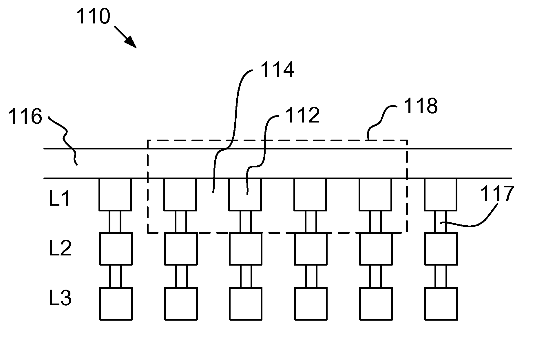
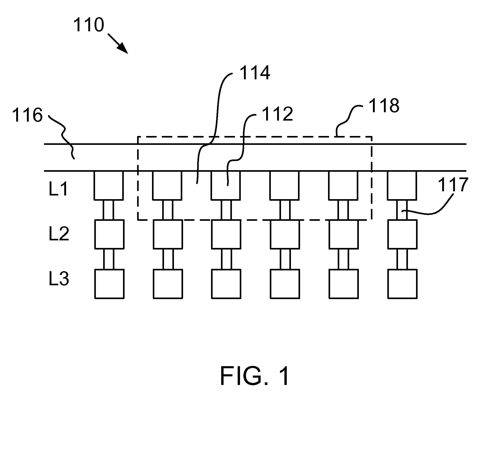
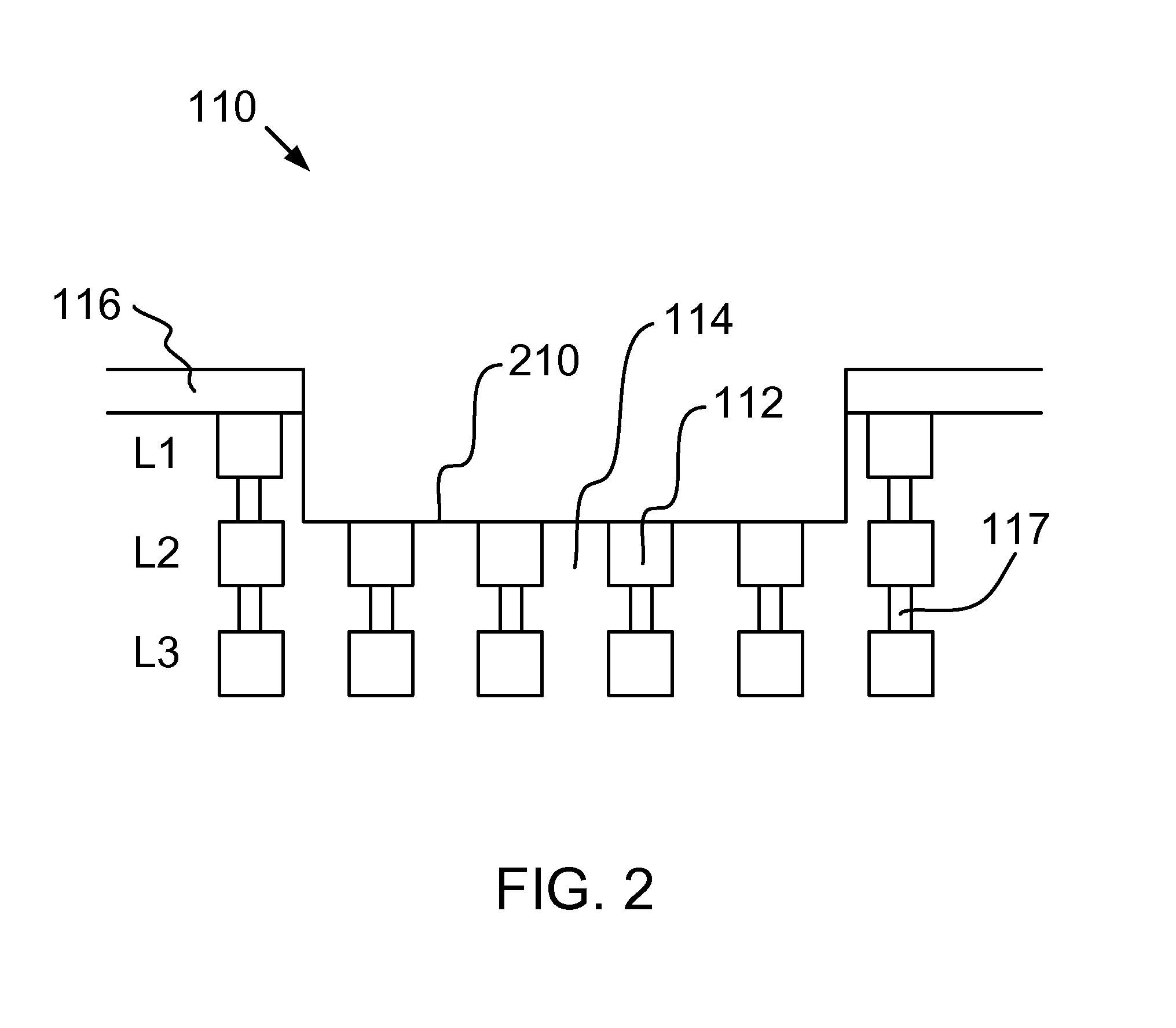
[0019]A preferred embodiment of this invention provides a method for uniformly removing multiple layers of mixed conductor and dielectric—such as the removal of multiple layers consisting of copper and low k dielectric—in a manner allowing access to the active features buried underneath these layers for applications including, but not limited to, circuit editing and failure analysis.

[0020]Preferred embodiments of the present invention are directed to a method used for milling of materials, particularly copper-based features within semiconductor devices. Although much of the following description is directed toward copper milling and specifically copper milling within semiconductor devices, the apparatus and methods of the present invention could equally be utilized in the milling of other materials. The techniques described herein can be used by themselves or in combination with other techniques. Hence, the scope of the present invention should not be limited to simply the milling o...


PUM

PropertyMeasurementUnit
Widthaaaaaaaaaa
Lengthaaaaaaaaaa
Dielectric polarization enthalpyaaaaaaaaaa

Abstract

A method and system for improved planar deprocessing of semiconductor devices using a focused ion beam system. The method comprises defining a target area to be removed, the target area including at least a portion of a mixed copper and dielectric layer of a semiconductor device; directing a precursor gas toward the target area; and directing a focused ion beam toward the target area in the presence of the precursor gas, thereby removing at least a portion of a first mixed copper and dielectric layer and producing a uniformly smooth floor in the milled target area. The precursor gas causes the focused ion beam to mill the copper at substantially the same rate as the dielectric. In a preferred embodiment, the precursor gas comprises methyl nitroacetate. In alternative embodiments, the precursor gas is methyl acetate, ethyl acetate, ethyl nitroacetate, propyl acetate, propyl nitroacetate, nitro ethyl acetate, methyl methoxyacetate, or methoxy acetylchloride.

Description

[0001]This application claims priority from U.S. Provisional Application 61 / 828,128, filed May 28, 2013, which is hereby incorporated by reference.TECHNICAL FIELD OF THE INVENTION[0002]The present invention relates to the field of charged particle beam processing and, in particular, to a method for uniformly removing multiple layers of conductor and dielectric from semiconductor circuits using a focused ion beam.BACKGROUND OF THE INVENTION[0003]Semiconductor devices such as microprocessors can be made up of millions of transistors, each interconnected by thin metallic lines branching over several levels and isolated electrically from each other by layers of dielectric materials. When a new semiconductor design is first produced in a semiconductor fabrication facility, it is typical to find that the design does not operate exactly as expected. It is then necessary for the engineers who designed the device to test their design and “rewire” it to achieve the desired functionality. Due ...

Claims


Application Information

Patent Timeline
IPC IPC(8): H01L21/3065H01L21/67
CPCH01L21/67069H01L21/3065H01J37/3056H01L21/32131H01J2237/3151H01J2237/31744H01J2237/31749H01L21/76892H01L21/31105H01L21/31116H01L21/32136H01J37/3233H01J37/3244H01J2237/334
Inventor RUE, CHADCHANDLER, CLIVE D.
Owner FEI CO
Why Eureka
Try Eureka