Method of manufacturing organic electroluminescence display device

a technology of electroluminescence display and organic electroluminescence, which is applied in the direction of solid-state devices, chemical vapor deposition coatings, coatings, etc., can solve the problems of process accuracy, pixel size has a limit of about 100 m, and stress may deform the opening in the mask, etc., to achieve high-efficiency, long-life, and high-definition

Inactive Publication Date: 2012-10-04
CANON KK
View PDF0 Cites 16 Cited by
  • Summary
  • Abstract
  • Description
  • Claims
  • Application Information

AI Technical Summary

Benefits of technology

[0009]The present invention has been made to solve the above-mentioned problems, and an object of the present invention is t

Problems solved by technology

However, in a metal mask, a vapor deposited film which adheres when vapor deposition operation is performed may narrow an opening in the mask or stress may deform the opening in the mask.
Therefore, it is necessary to clean the mask used after film formation for a fixed number of times, which is a disadvantageous factor from the viewpoint of manufacturing costs.
Further, partly due to a limitation on the process accuracy of the mask, the pixel size has a limit of about 100 μm, which is disadvantageous to a finer size.
However, when the stiffness of the mask is enhanced, an increase in the weight of the mask itself is caused accordingly.
Therefore, from the viewpoint of both processability and handling, it is difficult to manufacture large format display devices of the fourth and subsequent generations, and an optimum manufacturing process of a fine organic EL element and a display device havi

Method used


Image

  • Method of manufacturing organic electroluminescence display device
  • Method of manufacturing organic electroluminescence display device
  • Method of manufacturing organic electroluminescence display device

Examples


example 1

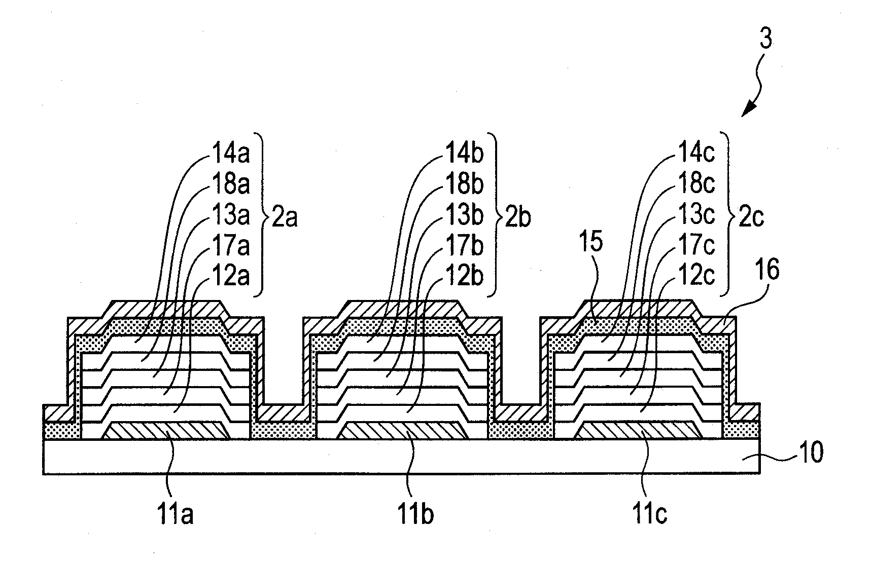
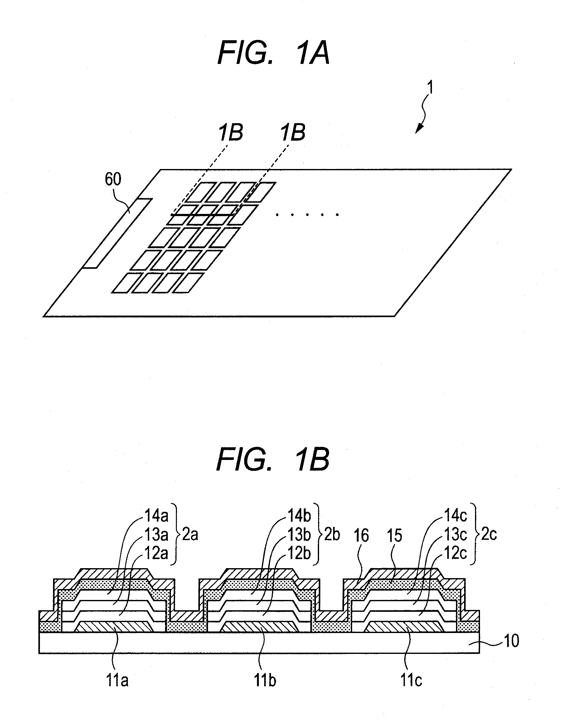
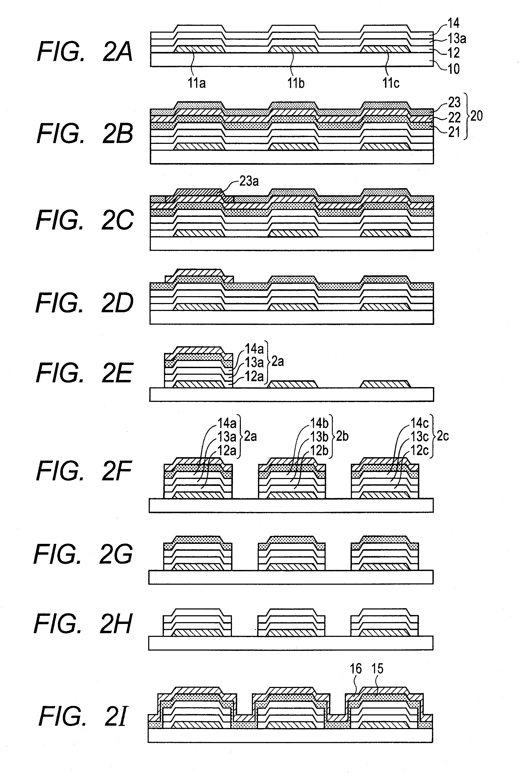
[0097]An organic EL display device 3 illustrated in FIG. 3 was manufactured according to manufacturing steps described in the following. Note that, in the organic EL display device 3 illustrated in FIG. 3, an electron blocking layer (17a, 17b, or 17c) is provided as an interposed layer between the hole transport layer (12a, 12b, or 12c) and the emission layer (13a, 13b, or 13c) in the organic EL display device 1 illustrated in FIGS. 1A and 1B. Further, a hole blocking layer (18a, 18b, or 18c) is provided as an interposed layer between the emission layer (13a, 13b, or 13c) and the electron transport layer (14a, 14b, or 14c). More specifically, each of the organic compound layers (2a, 2b, and 2c) is a laminate formed by laminating the hole transport layer, the electron blocking layer, the emission layer, the hole blocking layer, and the electron transport layer in the stated order. The basic flow of the manufacturing steps is the same as those illustrated in FIGS. 2A to 2I. Here, part...

example 2

[0130]An organic EL display device was manufactured in a way similar to that of Example 1 except that the step of removing the mask layer was also carried out in closed space. FIG. 5 is a schematic view illustrating a part of the organic EL display device used in this example (Example 2). An apparatus 40 illustrated in FIG. 5 includes, similarly to the apparatus 30 illustrated in FIG. 4, a delivery chamber 41, a drying chamber 42, a first film forming chamber 43, a second film forming chamber 44, an encapsulation operation chamber 45, and a transfer chamber 46, and in addition, includes a water-washing treatment chamber 47 for carrying out the step of removing the mask layer and a water dissipating chamber 48, and the water-washing treatment chamber 47 and the water dissipating chamber 48 are coupled to the delivery chamber 41. More specifically, the apparatus 40 illustrated in FIG. 5 includes multiple chambers including the water-washing treatment chamber 47, the water dissipating ...

example 3

[0132]An organic EL display device was manufactured in a way similar to that of Example 1 except that the step of forming the mask layer and the step of removing the mask layer were changed to steps described in the following. This example is described below.

[0133](A) Steps up to Step of Forming Mask Layer

[0134]The organic compound layer was formed on the substrate 10 in a way similar to that of Example 1. Note that, in this example, the electron transport layer 14 was formed so as to have a thickness of 50 nm.

[0135](B) Step of Forming Mask Layer

[0136]Next, a thin film of silicon nitride to be the mask layer 20 was formed on the organic compound layer.

[0137](C) Step of Forming Mask Layer

[0138]Next, by dry etching using a CF4 gas, the thin film to be the mask layer 20 was processed to form the mask layer 20. Note that, during the dry etching, a part of the electron transport layer 14 was etched by the CF4 gas, which could damage the electron transport layer itself. Therefore, through...


PUM

PropertyMeasurementUnit
Solubility (mass)aaaaaaaaaa

Abstract

Provided is a method of manufacturing an organic electroluminescence display device including an emission region, the emission region including multiple organic compound layers arranged therein, each of the organic compound layers being provided between a pair of electrodes and including at least an emission layer, the method including: forming in the entire emission region an organic compound layer which is insoluble in water; forming on the organic compound layer a mask layer containing a water-soluble material in a predetermined pattern; removing a part of the organic compound layer which is formed in a region which is not covered with the mask layer; removing the mask layer; drying the organic compound layer; and forming a common layer on the organic compound layers, in which the steps from the drying of the organic compound layer to the forming of a common layer are carried out in a vacuum.

Description

BACKGROUND OF THE INVENTION[0001]1. Field of the Invention[0002]The present invention relates to a method of manufacturing an organic electroluminescence (EL) display device and a manufacturing apparatus for carrying out the manufacturing method.[0003]2. Description of the Related Art[0004]A generally known display device having organic EL elements mounted thereon is a device in which pixels each having a single or multiple organic EL elements are arranged in a predetermined pattern. By those pixels, an emission region of the display device is two-dimensionally and finely divided. The organic EL elements included in the pixels are electronic elements which output, for example, any one of red light, green light, and blue light. A display device having organic EL elements mounted thereon obtains a full-color image by driving the organic EL elements for outputting desired colors at desired emission intensities.[0005]By the way, in an organic EL element which is a component of a display...

Claims


Application Information

Patent Timeline
IPC IPC(8): H01L51/40C23C16/56C23C16/02
CPCH01L27/3211H01L51/56H01L51/0017H01L51/0003H10K59/35H10K71/12H10K71/233H10K71/00
Inventor HIROKI, TOMOYUKIENDO, TAROTAKAYA, ITARUISHIGE, KOICHISATO, NOBUHIKO
Owner CANON KK
Why Eureka
Try Eureka