Seal ring structure and method of forming the same

Active Publication Date: 2014-12-11
MARLIN SEMICON LTD
View PDF2 Cites 5 Cited by
  • Summary
  • Abstract
  • Description
  • Claims
  • Application Information

AI Technical Summary

Benefits of technology

The present invention provides a method for forming a seal ring structure that prevents the formation of overhang defects in the conductive layer and enhances the structural completeness of the conductive layer. By modifying the gas ratio during the etching process, the opening is tilted or includes a concave-curved side, and the conductive layer filling the opening includes two convex-curved parts. Consequently, the overhang defect can be avoided, and the coverage rate of the second dielectric layer and the thickness uniformity of the film later formed by sputtering process can be further improved, leading to a more complete seal ring structure.

Problems solved by technology

However, with the trend of miniaturization of the electronic products, as the metal layer is predetermined to fill an opening partially exposing the interconnect layers, the small critical dimension of the interconnect layers may shrink the size of the opening, and the overhang defect may be formed during the formation of the metal layer, which may damage the thickness uniformity of the film such as a redistribution layer (RDL) that is later formed on the overall wafer through sputtering process.
Consequently, how to avoid the formation of the overhang defect in the metal layer of the protective structure is still an important issue in the field.

Method used


Image

  • Seal ring structure and method of forming the same
  • Seal ring structure and method of forming the same
  • Seal ring structure and method of forming the same

Examples


Embodiment Construction

[0015]To provide a better understanding of the present invention, preferred exemplary embodiments will be described in detail. The preferred exemplary embodiments of the present invention are illustrated in the accompanying drawings with numbered elements.

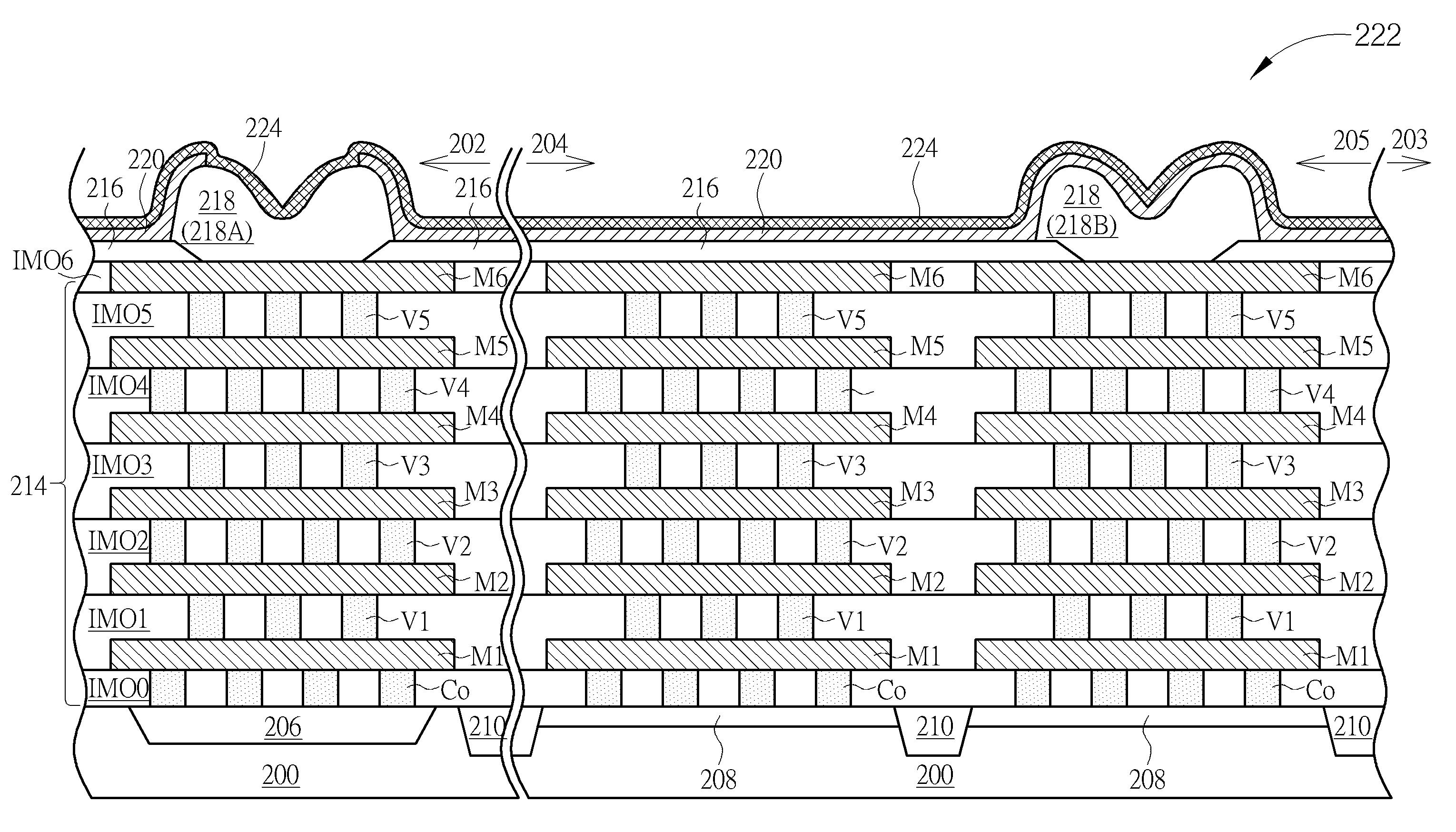
[0016]Please refer to FIG. 1 through FIG. 2, which are schematic diagrams illustrating a seal ring structure according to a first exemplary embodiment of the present invention. As shown in FIG. 1 and FIG. 2, the seal ring 10 includes a stack of metal / contact / via layers 14 (including metal layers M1-M6, via layers V1-V5, a contact metal layer Co, and inter-metal oxide layers IMO0-IMO6) disposed on the silicon substrate 12 in the seal ring region 28. Furthermore, a passivation layer 18 partially exposes the conductive layer 16 at the top, in which the exposed conductive layer 16 could be electrically connected to ground to enhance the insulation effect. A salicide layer 20 and a P+ doped region 22 are disposed below the contact metal...


PUM


Abstract

A method of forming a seal ring structure includes the following steps. A substrate is provided, and the substrate includes a seal ring region. A metal stack is formed in the seal ring region. A first dielectric layer covering the metal stack is formed. A part of the first dielectric layer is removed to form an opening to expose the metal stack, and at least a side of the opening is not perpendicular to a top surface of the first dielectric layer. A conductive layer is formed to fill the opening. A second dielectric layer is formed to continuously cover the first dielectric layer and the conductive layer, and the second dielectric layer has a v-shaped surface totally overlapping the conductive layer.

Description

BACKGROUND OF THE INVENTION[0001]1. Field of the Invention[0002]The present invention relates to a method of forming a seal ring structure, and more particularly, to a method of forming a seal ring structure having a v-shaped dielectric layer conformally and totally overlapping a conductive layer, which may serve as a protective structure for an integrated circuit region.[0003]2. Description of the Prior Art[0004]In order to protect a region of a semiconductor device in which an integrated circuit is formed (hereinafter referred to as an “integrated circuit (IC) region”) from being affected by moisture and ions contained in an ambient air, a protective structure called a “seal ring”, “die edge seal”, or “guard ring” is provided on an inner side of a scribe line, that is, in the vicinity of an edge portion of a chip (die). In a high-productivity process, a typical seal ring is formed of interconnect layers and contacts made of materials in the same manner as the integrated circuit (I...

Claims


Application Information

Patent Timeline
IPC IPC(8): H01L23/58H01L21/768
CPCH01L23/585H01L21/76877H01L21/76802H01L23/564H01L2924/0002
Inventor ZENG, FAN-QINGTEY, CHING HWAXU, XIAOQING
Owner MARLIN SEMICON LTD
Why Eureka
Try Eureka