Vertical cavity surface emitting laser device having a higher optical output power

a laser device and vertical cavity technology, applied in semiconductor lasers, optical resonator shapes and constructions, active medium materials, etc., can solve the problems of reducing the optical output power, p-type algaas has a disadvantage in optical output power, and the active layer generally suffers from a lower lasing power

Inactive Publication Date: 2006-08-31
FURUKAWA ELECTRIC CO LTD
View PDF14 Cites 7 Cited by
  • Summary
  • Abstract
  • Description
  • Claims
  • Application Information

AI Technical Summary

Benefits of technology

[0025] In accordance with the VCSEL device of the present invention, since the tunnel junction layers have a superior crystallinity and a reduced residual strain, a long-wavelength-range VCSEL device having a higher reliability can be obtained. In addition, since the band profile of the tunnel junction layers can be optimized, the resultant VCSEL device has a lower device resistance and superior temperature characteristics. Moreover, a larger diameter can be employed for the emission aperture without degrading the single-mode transverse lasing characteristic, thereby providing a VCSEL device having a higher optical output power /

Problems solved by technology

In a 0.85-μm-range VCSEL device, since p-type AlGaAs used as the material for the p-type semiconductor reflector incurs a large optical loss due to absorption in the valence band, the p-type AlGaAs has a disadvantage in the optical output power if used in a long-wavelength-range VCSEL device, in which the active layer generally suffers from a lower lasing power.
In particular, the problem therein is that a higher ambient temperature markedly reduces the optical output power.

Method used


Image

  • Vertical cavity surface emitting laser device having a higher optical output power
  • Vertical cavity surface emitting laser device having a higher optical output power
  • Vertical cavity surface emitting laser device having a higher optical output power

Examples


first embodiment

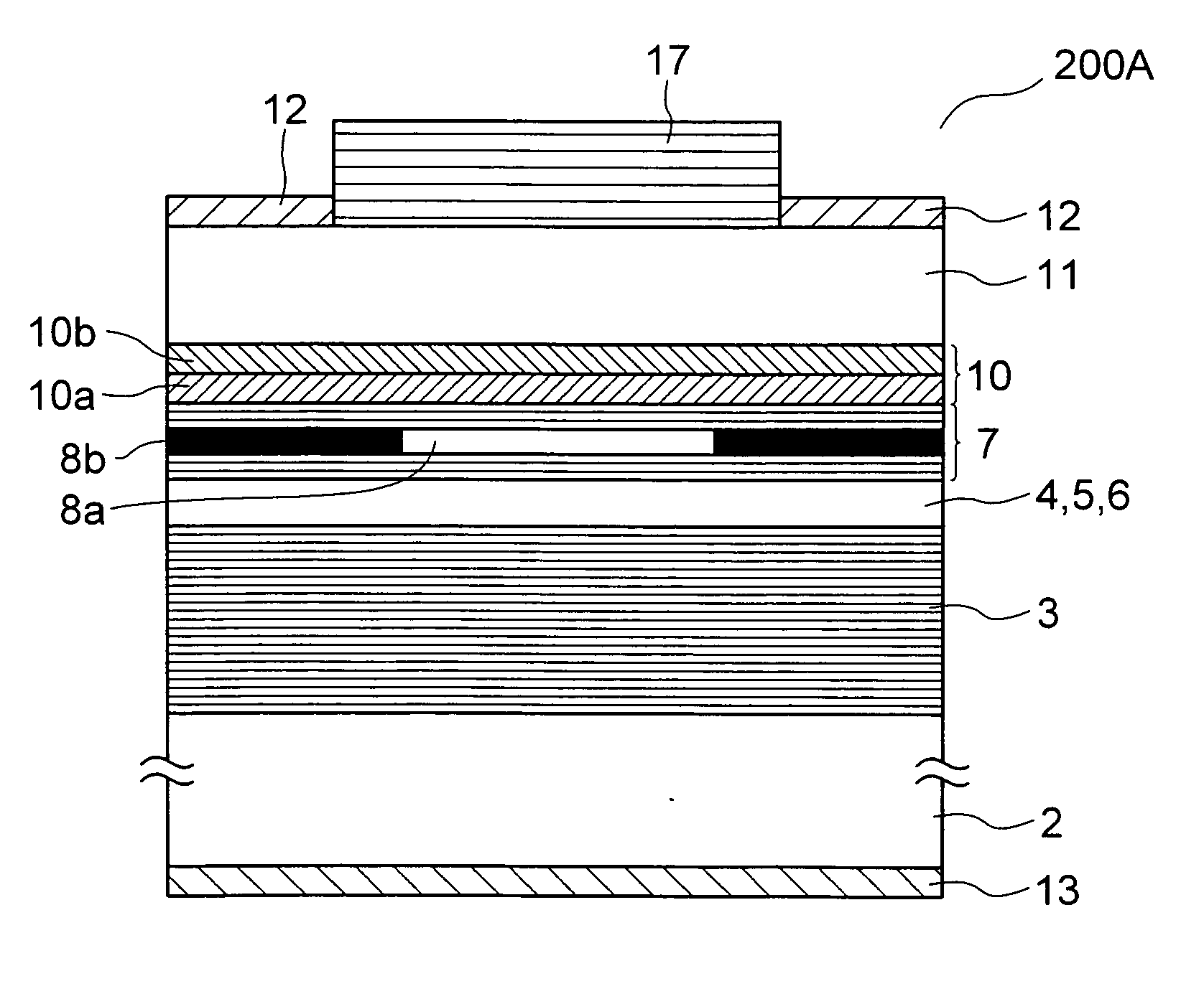
[0033] The first embodiment of the present invention is directed to a tunnel-junction VCSEL device of an oxidized-confinement type having an emission wavelength of 1290 nm and including an oxide aperture.

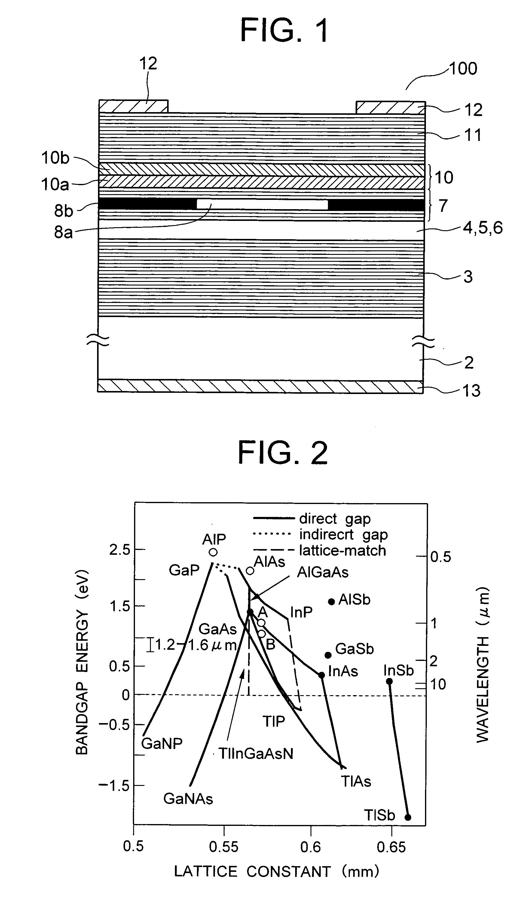
[0034]FIG. 1 shows a longitudinal-sectional view of the VCSEL device of the first embodiment. The VCSEL device 100 includes an n-GaAs substrate 2, and an epitaxial layer structure including an n-type bottom multilayer semiconductor reflector 3, a 125-nm-thick n-GaAs lower cladding layer 4, a MQW active layer structure 5, a 125-nm-thick p-GaAs upper cladding layer 6, p-type multilayer film 7, tunnel junction layers 10, a top multilayer semiconductor reflector 11, which are consecutively deposited on the n-GaAs substrate 2.

[0035] The n-type bottom multilayer reflector 3 includes n-Al0.9Ga0.1As layers and n-GaAs layers each having a thickness of ¼ optical length and alternately deposited in pair to form 35 layer pairs. The MQW active layer film 5 includes a plurality of 6-nm-thick qu...

second embodiment

[0042] The second embodiment of the present invention is directed to a tunnel-junction VCSEL device of an oxidized-confinement type having an emission wavelength of 1300 nm. The VCSEL device of the present embodiment is similar to the first embodiment except for the composition of the tunnel junction layers, and thus will be also described with reference to FIG. 1.

[0043] The tunnel junction layers 10 in the present embodiment includes a p++-Ti0.02In0.02Ga0.96As0.945N0.005Sb0.05 layer 10a doped with carbon at a concentration of 1×1020 cm−3 and an n++-Ti0.02In0.02Ga0.96As0.975N0.02Sb0.005 layer 10b doped with silicon at a concentration of 1×1019 cm−3. The p++-type layer 10a is in contact with the underlying p-type multilayer film 7.

[0044] The Sb included in both the n++- and p++-type layers 10b, 10a improves the crystallinity of the tunnel junction layers 10 due to the surfactant effect thereof during the epitaxial growth of the tunnel junction layers 10. The N included in both the ...

third embodiment

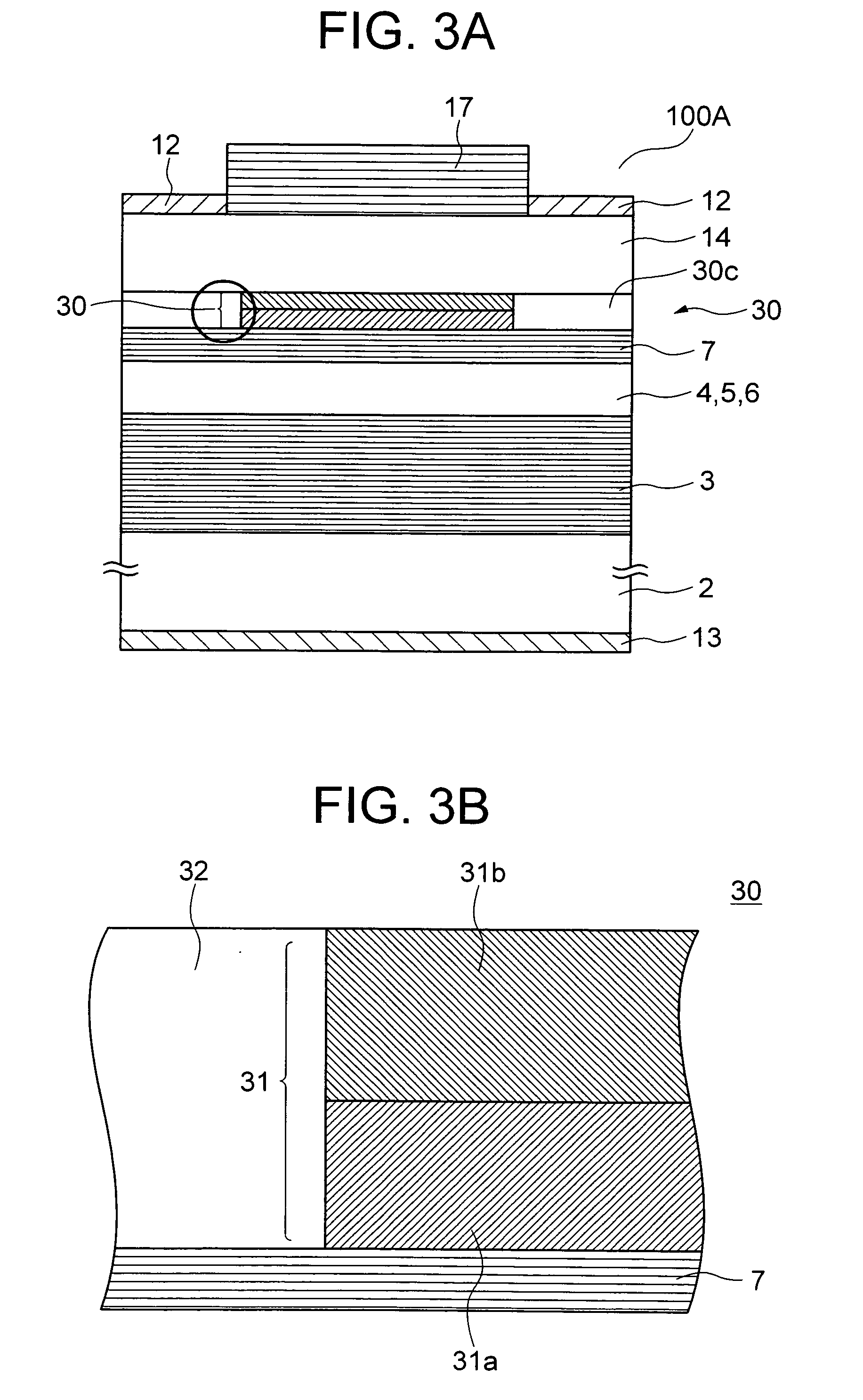
[0049] The third embodiment of the present invention is directed to a tunnel-junction VCSEL device having an emission wavelength of 1305 nm. Referring to FIG. 3A, the VCSEL device 100A of the present embodiment includes an n-GaAs substrate 2, and an epitaxial layer structure including an n-type bottom multilayer semiconductor reflector 3, a 126-nm-thick n-GaAs lower cladding layer 4, a MQW active layer structure 5, a 126-nm-thick p-GaAs upper cladding layer 6, a p-type multilayer film 7, a tunnel junction / current confinement structure 30, and an n-GaAs contact layer 14, which are consecutively deposited on the n-GaAs substrate 2. The n-type bottom multilayer reflector 3 includes n-Al0.9Ga0.1As layers and n-GaAs layers each having a thickness of ¼ optical length and alternately deposited in pair to form 35 layer pairs. The MQW active layer structure 5 includes a plurality of 6-nm-thick Ga0.67In0.33N0.01As0.99 quantum well (QW) layers and a plurality of GaN0.019As0.081 barrier layers ...


PUM


Abstract

A vertical cavity surface emitting laser (VCSEL) device includes has an epitaxial layer structure formed on a GaAs substrate and including a pair of multilayer reflectors and a tunnel junction structure. The tunnel junction structure is configured by a heavily-doped n-type Tix2Inx1Ga1-x1-x2As1-y1-y2Ny1Sby2 mixed-crystal layer and a heavily-doped p-type Tix4Inx3Ga1-x3-x4As1-y3-y4Ny3Sby4 mixed-crystal layer, where 0≦x2≦0.3, 0≦x1≦0.3, 0<y1≦0.05, 0<y2≦0.3, 0≦x4≦0.3, 0≦x3≦0.05, 0<y3≦0.05, and 0<y4≦0.3.

Description

TECHNICAL FIELD [0001] The present invention relates to a vertical cavity surface emitting laser (VCSEL) device. BACKGROUND ART [0002] VCSEL devices have advantages that a plurality of VCSEL devices can be arranged in a two dimensional array on a single common substrate and operate with a lower threshold current, and thus are suited for use in the field of optical interconnection, optical computing and optical communication. [0003] The VCSEL devices can be manufactured at a lower cost and are now to replace the DFB (distributed feedback) laser devices which have been used heretofore as a light source in the fields of middle- to long-distance optical communications. For the purpose of application in these fields, it is necessary to develop an improved VCSEL device having a longer emission wavelength of 0.85 μm or longer and capable of lasing in a single transverse mode. [0004] A long-wavelength-range VCSEL device having a GaInNAs quantum well layer and lasing at a wavelength of 1.2 μ...

Claims


Application Information

Patent Timeline
Patent Type & Authority Applications(United States)
IPC IPC(8): H01S3/14H01S5/20H01S5/00H01S3/08H01S5/323
CPCB82Y20/00H01S5/18308H01S5/18311H01S5/18369H01S5/3095H01S5/32366H01S5/34306H01S2301/166
Inventor CASIMIRUS, SETIAGUNGKAGEYAMA, TAKEO
Owner FURUKAWA ELECTRIC CO LTD
Why Eureka
Try Eureka