Method for evaluating silicon single crystal and method for manufacturing silicon single crystal

a silicon single crystal and single crystal technology, applied in the direction of semiconductor/solid-state device testing/measurement, after-treatment details, instruments, etc., can solve the problems of reducing the concentration of silicon single crystal, increasing the cost, and shifting the resistivity of the substrate, so as to achieve high accuracy and enhance the effect of versatility

Active Publication Date: 2014-12-11
SHIN-ETSU HANDOTAI CO LTD
View PDF6 Cites 3 Cited by
  • Summary
  • Abstract
  • Description
  • Claims
  • Application Information

AI Technical Summary

Benefits of technology

[0033]As described above, the method for evaluating silicon single crystal according to the present invention can be extensively applied to not only silicon single crystal of high oxygen concentration but also the same of low oxygen concentration, the versatility can be enhanced, and the evaluation can be highly accurately performed as compared with conventional examples.
[0034]Furthermore, the method for manufacturing silicon single crystal according to the present invention enables growing and manufacturing the silicon single crystal while considering an amount of carriers generated due to oxygen donors by the heat treatment, and hence a product having a desired resistivity can be finally obtained.

Problems solved by technology

However, when a high-resistivity substrate of crystal grown by the CZ method is used, there occurs a problem that oxygen atoms that are present in CZ crystal form oxygen donors by a heat treatment at a relative low temperature for wiring or packaging which is a post-process of a device and thereby a resistivity of the substrate shifts.
However, according to this method, there is a problem that a high-temperature heat treatment process is required and hence costs are increased.
However, as described in Patent Literature 3 or the like, a top side (a head side) of crystal generally has high oxygen concentration, lowering this concentration is difficult, and hence an good chip yield is decreased as the target oxygen concentration that should be achieved becomes lower.
Furthermore, when the target oxygen concentration is extremely low, material melt in the crucible starts to be solidified and dislocation of crystal occurs in some cases.
Therefore, if the considerably low oxygen concentration is aimed, there occurs a problem that costs increase in the end.

Method used


Image

  • Method for evaluating silicon single crystal and method for manufacturing silicon single crystal
  • Method for evaluating silicon single crystal and method for manufacturing silicon single crystal
  • Method for evaluating silicon single crystal and method for manufacturing silicon single crystal

Examples


experiment 1

[0082]First, the relational expression Δ[C]=α′[Oi]3×exp(−β′·D(T)·[Oi]·t) (where α′ and β′ are constants) derived from International Publication No. WO 2005 / 071144 and the like described above will be examined.

[0083]Like Step 1, P-type crystal having oxygen concentration distributed thereto is grown by using the CZ method and the MCZ method, and wafer-shaped samples were sliced out from this grown crystal.

[0084]Samples having the oxygen concentrations [Oi]=9.2×10¹⁷, 10.8×10¹⁷, 12.8×10¹⁷, 13.8×10¹⁷, and 15.9×10¹⁷ atoms / cm3 (ASTM' 79) were prepared.

[0085]Then, each sample was subjected to a donor killer heat treatment, then a PN determination and measurement of a resistivity. Subsequently, samples were divided into two groups and subjected to a heat treatment at 450° facilitating generation of oxygen donors on two levels, i.e., one hour (3600 seconds) and 15 hours (54000 seconds), respectively. Each sample was again subjected to the PN determination and the measurement of a resistivity...

experiment 2

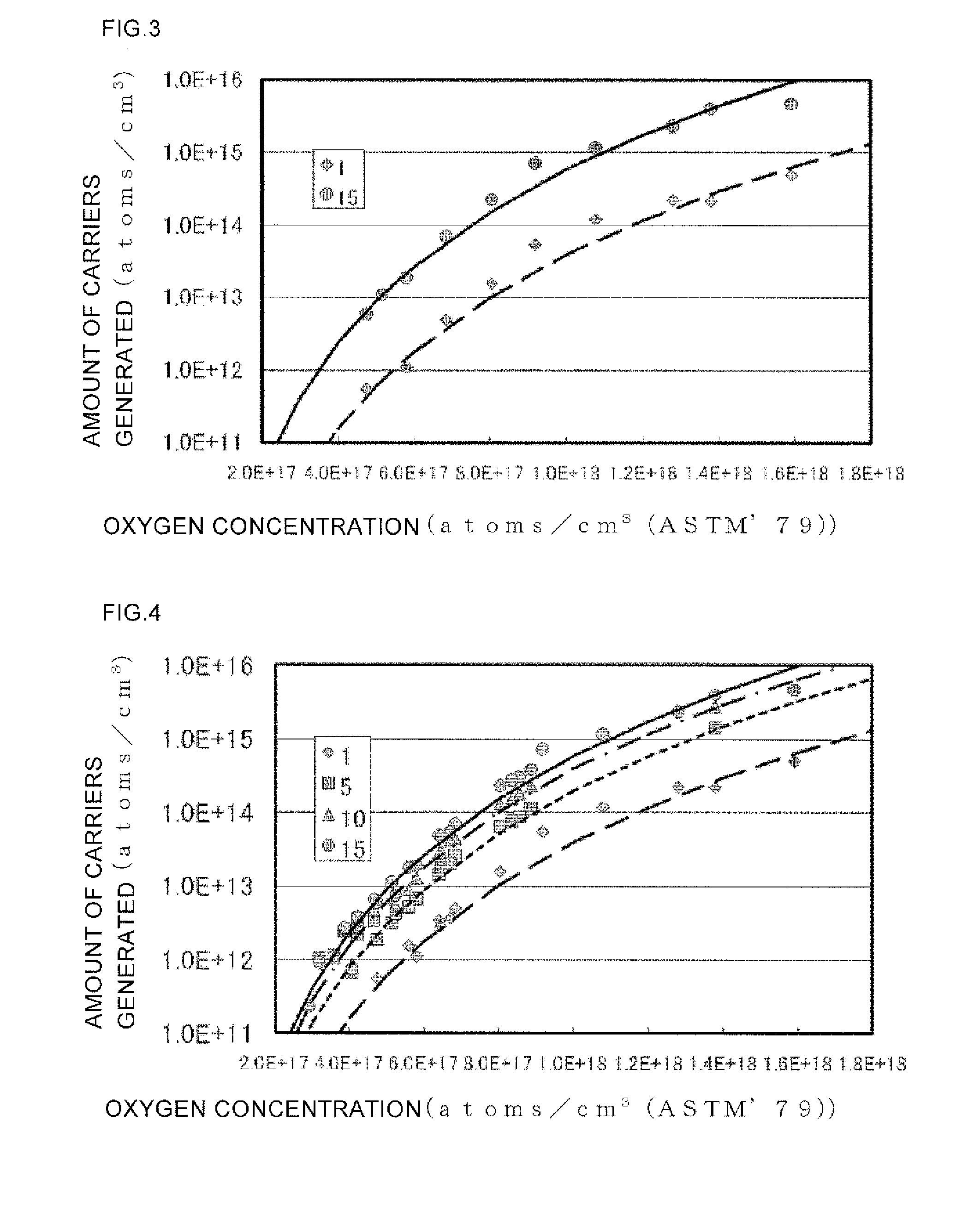
[0090]Subsequently, whether Expression (1) could be used even in an extended lower oxygen concentration region was confirmed.

[0091]Like Experiment 1, samples each having oxygen concentration distributed thereto were prepared. However, oxygen levels are lower than those in Experiment 1, and they are 4.8×10¹⁷, 5.2×10¹⁷, 5.8×10¹⁷, 6.8×10¹⁷, and 8.0×10¹⁷ atoms / cm3 (ASTM' 79). Since the oxygen concentration must be lowered, the samples used here were all fabricated by using the MCZ method with a magnetic field applied.

[0092]These samples were subjected to the donor killer heat treatment, then the PN determination and the measurement of a resistivity. Subsequently, the heat treatment was carried out at 450° C. for one hour and for 15 hours, and the PN determination and the measurement of a resistivity were again performed in a completely the same manner as Experiment 1. Based on obtained results, an amount of carriers generated due to oxygen donors was obtained and plotted in FIG. 10 with...

experiment 3

[0095]However, using MCZ crystal in a low-oxygen concentration region that was not observed in the prior art can be expected, and hence an expression that can also represent a low-oxygen concentration side is preferable. Thus, an expression that substitutes for Expression (1) and enables obtaining an amount of carriers generated due to oxygen donors was keenly examined based on these pieces of data.

[0096]As a result, it was revealed that the following expression can be used with respect to the silicon single crystal in each of Experiments 1 and 2.

Δ[C]=5.78×10−74×[Oi]5×exp(−6.25×10⁻⁷×D(T)·[Oi]·t)   Expression (2)

[0097]Specifically, on the low-oxygen concentration side in FIG. 10, experimental results (points) do not coincide with Δ[C]=4.53×10−39×[Oi]3×exp(−1.63×10⁻⁵×D(T)·[Oi]·t) (a line) of Expression (1) obtained in the experiment 1. When the oxygen concentration becomes lowered, the experimental values rapidly become smaller than Expression (1). Therefore, it is assumed that an inf...


PUM

PropertyMeasurementUnit
temperatureaaaaaaaaaa

Abstract

The present invention provides a method for evaluating silicon single crystal wherein an amount Δ[C] of carriers generated due to oxygen donors produced when a heat treatment is performed to the silicon single crystal is calculated and evaluated, the amount Δ[C] being calculated from oxygen concentration [Oi] in the silicon single crystal, a temperature T of the heat treatment, a time t of the heat treatment, and an oxygen diffusion coefficient D(T) at the temperature T by using the following relational expression:Δ[C]=α[Oi]5×exp(−β·D(T)·[Oi]·t) (where α and β are constants). As a result, there is provided a method that enables evaluating an amount of carriers generated due to oxygen donors in silicon single crystal in a further versatile manner.

Description

TECHNICAL FIELD[0001]The present invention relates to a method for evaluating silicon single crystal and a method for manufacturing silicon single crystal, and more particularly to a method for evaluating silicon single crystal containing oxygen grown by a Czochralski method (a CZ method), a magnetic field applied Czochralski method (an MCZ method), or the like and a method for manufacturing the same.BACKGROUND ART[0002]In mobile communications as typified by a mobile phone or the like, low costs, high integration, low power, multifunction, speed improvement, and others evolve day by day. So-called RF (radio frequency) devices are used in these aspects. A compound semiconductor is exclusively used for such RF devices.[0003]However, in recent years, since a CMOS process has been finer or a reduction in cost is desired, an RF device based on silicon has become feasible.[0004]In an RF device using a silicon single crystal wafer, when a substrate resistivity is low, loss is high because...

Claims


Application Information

Patent Timeline
Patent Type & Authority Applications(United States)
IPC IPC(8): H01L21/322H01L21/66
CPCH01L22/12H01L21/3225C30B29/06C30B15/00C30B33/02
Inventor HOSHI, RYOJIKAMADA, HIROYUKIMATSUMOTO, SUGURU
Owner SHIN-ETSU HANDOTAI CO LTD
Why Eureka
Try Eureka