Semiconductor Device and Manufacturing Method Thereof
Active Publication Date: 2014-12-25
SEMICON ENERGY LAB CO LTD
View PDF3 Cites 21 Cited by
Summary
Abstract
Description
Claims
Application Information
AI Technical Summary
This helps you quickly interpret patents by identifying the three key elements:
Problems solved by technology
Method used
Benefits of technology
Benefits of technology
The patent text discusses the problem of impurities in wiring materials causing poor electrical characteristics of transistors, and proposes a solution to improve the reliability of semiconductor devices that contain copper, aluminum, gold, or silver wiring. The invention includes the use of protective layers to prevent impurities from entering the semiconductor layer and increase the resistance of the layer. The protective layers can be formed without increasing the number of photomasks, resulting in a highly reliable semiconductor device with high productivity.
Problems solved by technology
However, there are problems in that copper, aluminum, gold, silver, or the like, which is a constituent element of the wiring, is difficult to process, and they are diffused in a semiconductor layer in the processing.
Copper, aluminum, gold, silver, and the like, which are constituent elements of the wiring, are impurities causing poor electrical characteristics of a transistor.
Therefore, there is a problem in that entry of the impurities into the semiconductor layer reduces the resistance of the semiconductor layer and the amount of change in electrical characteristics, typically in threshold voltage, of the transistor is increased by change over time or a stress test.
Method used
Image
Click on the blue label to locate the original text in one second.
Reading with bidirectional positioning of images and text.
Examples
embodiment 1
[0048]In this embodiment, a structure and a manufacturing method of a semiconductor device of one embodiment of the present invention will be described with reference to FIGS. 1A to 1D, FIGS. 2A to 2D, FIGS. 3A to 3D, and FIGS. 4A to 4E.
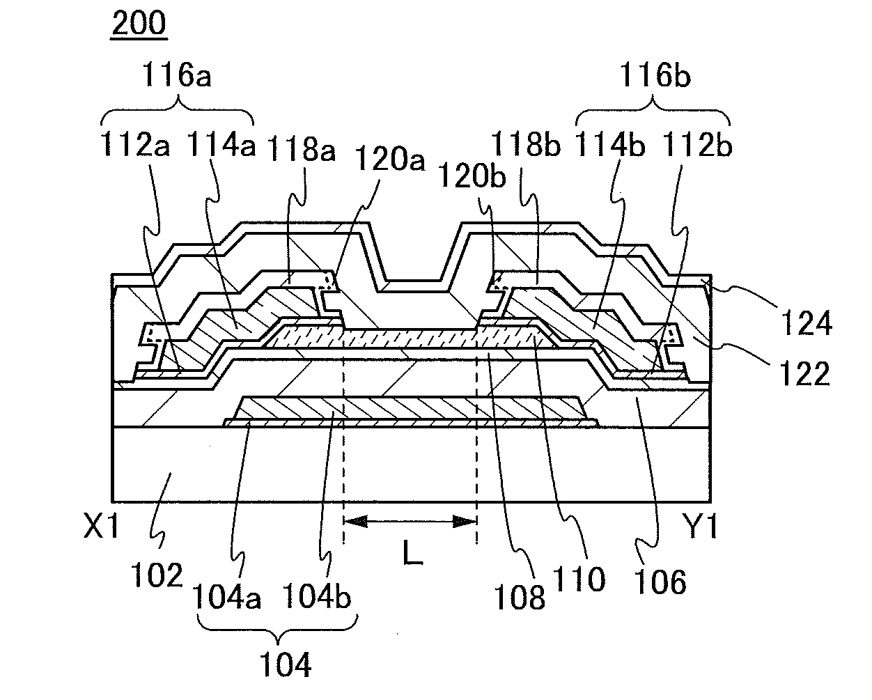
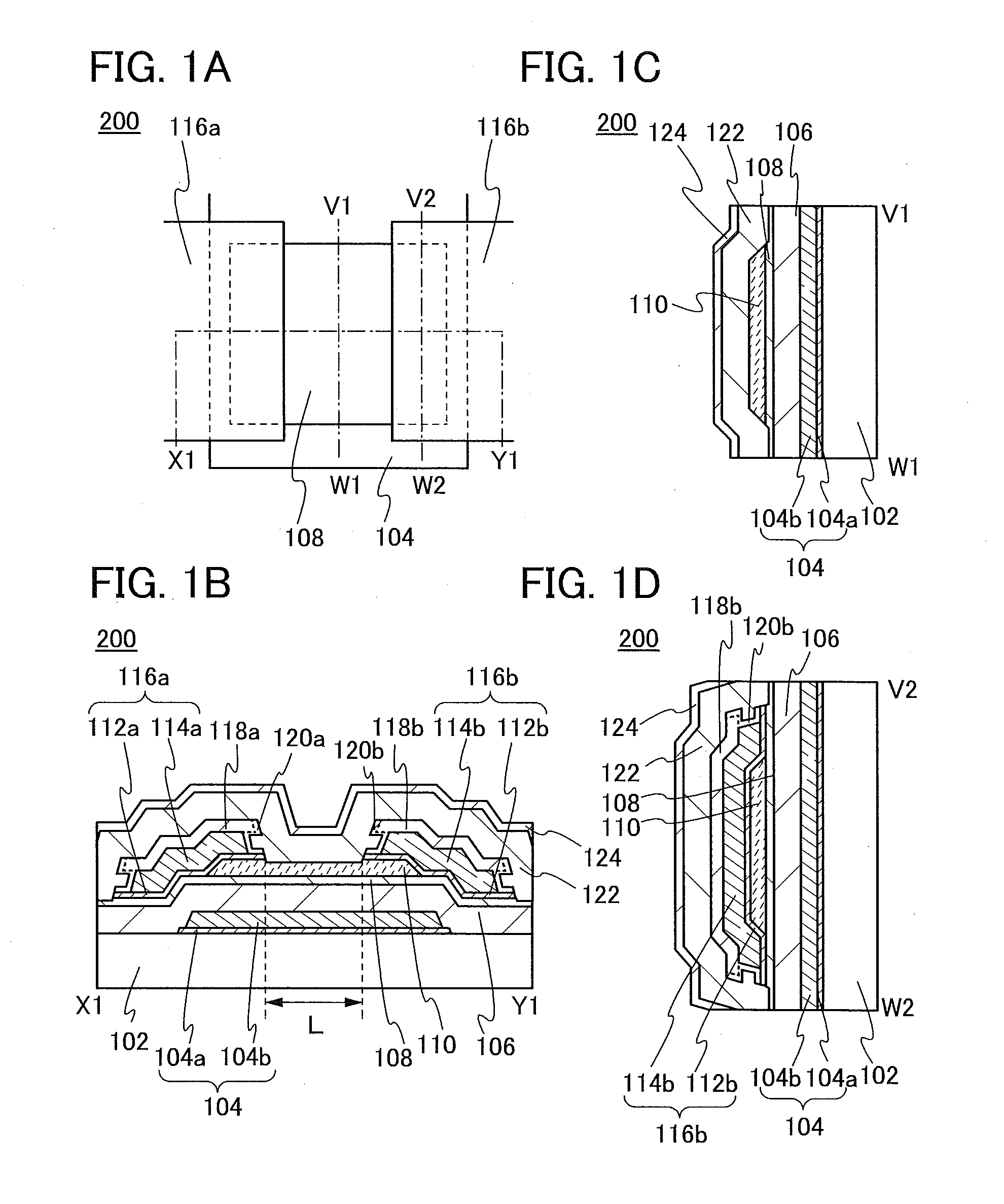
[0049]FIGS. 1A to 1D illustrate a structure example of a transistor 200 included in a semiconductor device. FIG. 1A is a plan view of the transistor 200. FIG. 1B is a cross-sectional view taken along dashed-dotted line X1-Y1 in FIG. 1A. FIG. 1C is a cross-sectional view taken along dashed-dotted line V1-W1 in FIG. 1A. FIG. 1D is a cross-sectional view taken along dashed-dotted line V2-W2 in FIG. 1A. Note that some components (e.g., an insulating film 124) of the transistor 200 are not illustrated in FIG. 1A for simplicity.
[0050]The transistor 200 in FIGS. 1A to 1D includes a gate electrode 104 over a substrate 102, insulating films 106 and 108 over the gate electrode 104, a semiconductor layer 110 overlapping the gate electrode 104 with the insulatin...
embodiment 2
[0177]In this embodiment, a structure of a semiconductor device of one embodiment of the present invention, which is different from that in Embodiment 1, will be described. Note that Embodiment 1 can be referred to for the portion similar to that in Embodiment 1 and detailed description of the portion is omitted.
[0178]FIGS. 5A to 5C show a transistor 230 included in a semiconductor device of this embodiment. FIG. 5A is a plan view of the transistor 230, FIG. 5B is a cross-sectional view taken along dashed-dotted line X4-Y4 in FIG. 5A, and FIG. 5C is a cross-sectional view taken along dashed-dotted line V7-W7 in FIG. 5A. Note that some components (e.g., the insulating film 124) of the transistor 230 are not illustrated in FIG. 5A for simplicity.
[0179]The transistor 230 in FIGS. 5A to 5C is a channel-etched transistor and includes the gate electrode 104 over the substrate 102, the insulating films 106 and 108 over the gate electrode 104, the semiconductor layer 110 overlapping the gat...
embodiment 3
[0196]In this embodiment, a semiconductor device having a transistor in which an oxide semiconductor layer is used as a semiconductor layer and the number of defects in the oxide semiconductor layer can be reduced is described with reference to drawings. Transistors described in this embodiment are different from those in Embodiment 1 or 2 in that the transistor of this embodiment includes a multilayer film including a plurality of oxide semiconductor layers. Here, details of the transistors are described using the semiconductor device shown in FIGS. 1A to 1D in Embodiment 1.
[0197]FIGS. 6A to 6D are a top view and cross-sectional views of a transistor 210 included in a semiconductor device.
[0198]FIG. 6A is a plan view of the transistor 210. FIG. 6B is a cross-sectional view taken along dashed-dotted line X2-Y2 in FIG. 6A. FIG. 6C is a cross-sectional view taken along dashed-dotted line V3-W3 in FIG. 6A. FIG. 6D is a cross-sectional view taken along dashed-dotted line V4-W4 in FIG. 6...
PUM
Abstract
To improve the reliability of a semiconductor device including a low-resistance material such as copper, aluminum, gold, or silver as a wiring. Provided is a semiconductor device including a pair of electrodes electrically connected to a semiconductor layer which has a stacked-layer structure including a first protective layer in contact with the semiconductor layer and a conductive layer containing the low-resistance material and being over and in contact with the first protective layer. The top surface of the conductive layer is covered with a second protective layer functioning as a mask for processing the conductive layer. The side surface of the conductive layer is covered with a third protective layer. With this structure, entry or diffusion of the constituent element of the pair of conductive layers containing the low-resistance material into the semiconductor layer is suppressed.
Description
BACKGROUND OF THE INVENTION[0001]1. Field of the Invention[0002]One embodiment of the invention disclosed in this specification relates to a semiconductor device and a manufacturing method thereof.[0003]2. Description of the Related Art[0004]Transistors used for most flat panel displays typified by liquid crystal display devices and light-emitting display devices are formed using silicon semiconductors such as amorphous silicon, single crystalsilicon, and polycrystalline silicon provided over glass substrates. Further, such a transistor employing such a silicon semiconductor is used in integrated circuits (ICs) and the like.[0005]Further, the increase in size and definition of a flat panel display increases the driving frequency, the resistance, and the parasitic capacitance of a wiring, leading to wiring delay. In order to inhibit the wiring delay, a technique for forming a wiring using a low-resistance material such as copper, aluminum, gold, and silver has been studied (Patent D...
Claims
Application Information
Patent Timeline
Application Date:The date an application was filed.
Publication Date:The date a patent or application was officially published.
First Publication Date:The earliest publication date of a patent with the same application number.
Issue Date:Publication date of the patent grant document.
PCT Entry Date:The Entry date of PCT National Phase.
Estimated Expiry Date:The statutory expiry date of a patent right according to the Patent Law, and it is the longest term of protection that the patent right can achieve without the termination of the patent right due to other reasons(Term extension factor has been taken into account ).
Invalid Date:Actual expiry date is based on effective date or publication date of legal transaction data of invalid patent.

