HEMT Structure with Iron-Doping-Stop Component and Methods of Forming

a technology of hemt and components, applied in the direction of basic electric elements, electrical equipment, semiconductor devices, etc., can solve the problems of limited control of doping concentration, severe delay in the profile of iron doping across intentionally-doped buffer layers, and limited effectiveness of intentionally-doped buffer layers, so as to reduce the mobility of iron atoms floating, reduce or eliminate contamination of channel layers, and minimize or eliminate any degradation of hemt characteristics

Active Publication Date: 2015-01-01
IQE KC
View PDF1 Cites 14 Cited by
  • Summary
  • Abstract
  • Description
  • Claims
  • Application Information

AI Technical Summary

Benefits of technology

[0008]This invention has many advantages. For example, the inventors have discovered that, by lowering the growth temperature of a buffer layer from a temperature in a range of between about 900° C. and about 1100° C. to a temperature in a range of between about 500° C. and about 900° C., the consequent low-growth temperature reduces mobility of the iron atoms floating on the surface of gallium nitride being deposited and, consequently, forces them to become incorporated into the iron-doping stop layer being deposited. Without being limited to any particular theory, it is believed that, if sufficiently thick, the iron-doping stop layer grown at low temperature w

Problems solved by technology

The effectiveness of intentionally-doped buffer layers is often limited by the limited ability to control the concentration of doping during fabrication of the buffer layer.
In particular, the profile of iron doping across an intentionally-doped buffer layer exhibits severe delay and a slow rise in the concentration of the iron upon introduction of iron during deposition of the layer and also very

Method used


Image

  • HEMT Structure with Iron-Doping-Stop Component and Methods of Forming
  • HEMT Structure with Iron-Doping-Stop Component and Methods of Forming
  • HEMT Structure with Iron-Doping-Stop Component and Methods of Forming

Examples


Embodiment Construction

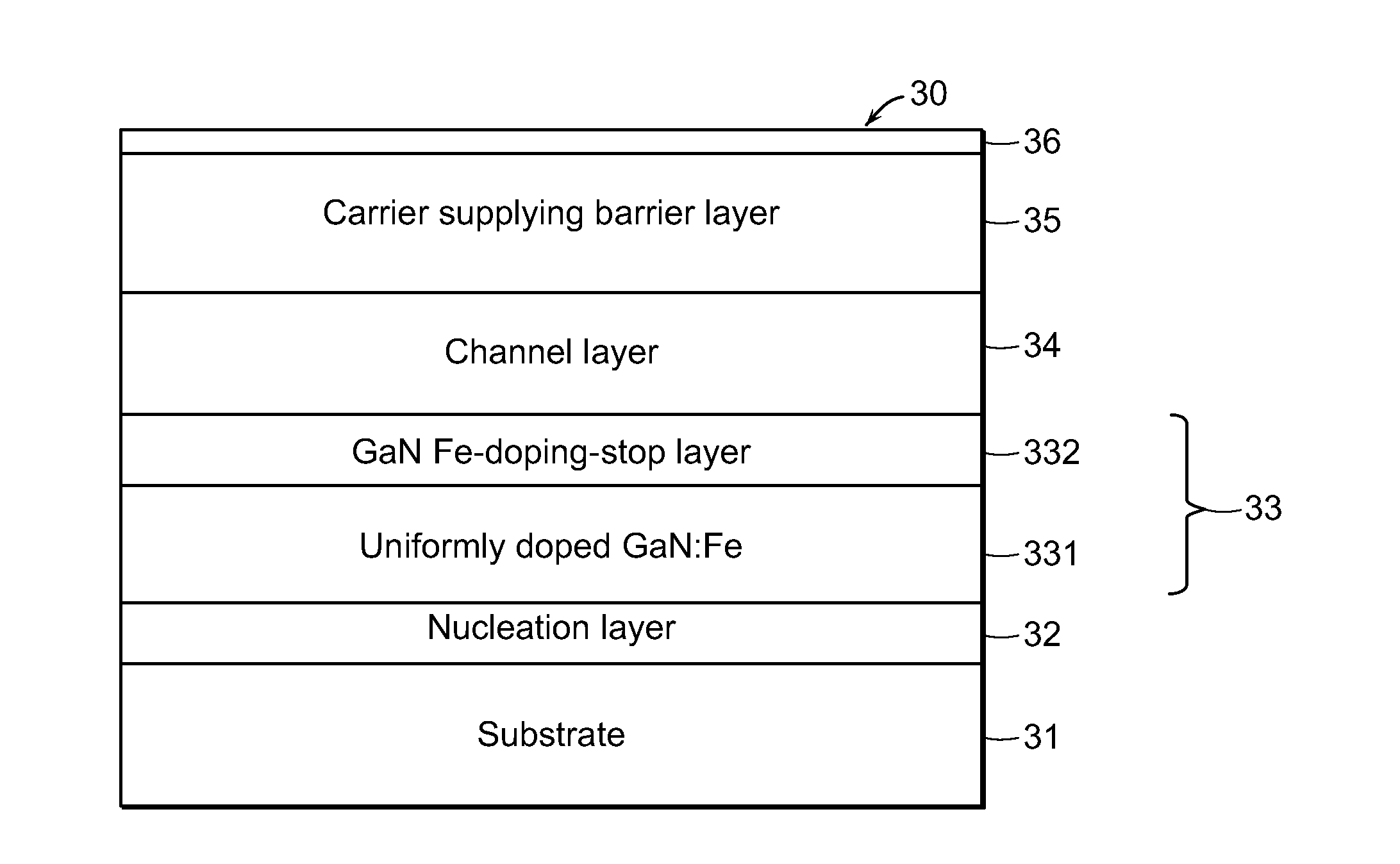
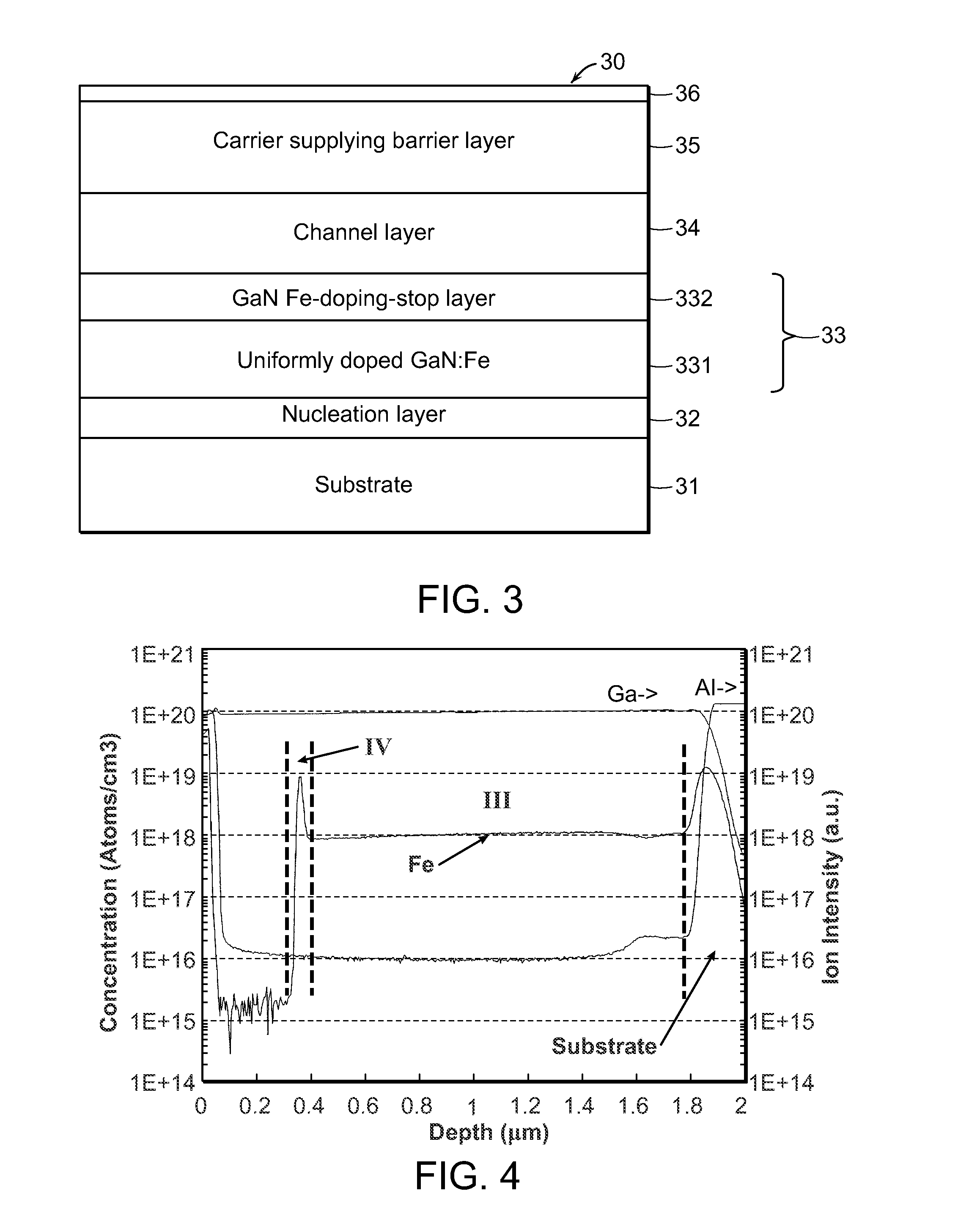
[0015]The invention is directed to an iron-doped high electron-mobility transistor (HEMT) structure that includes a GaN buffer layer that includes an iron-doping-stop layer, and to a method of forming the HEMT structure of the invention.

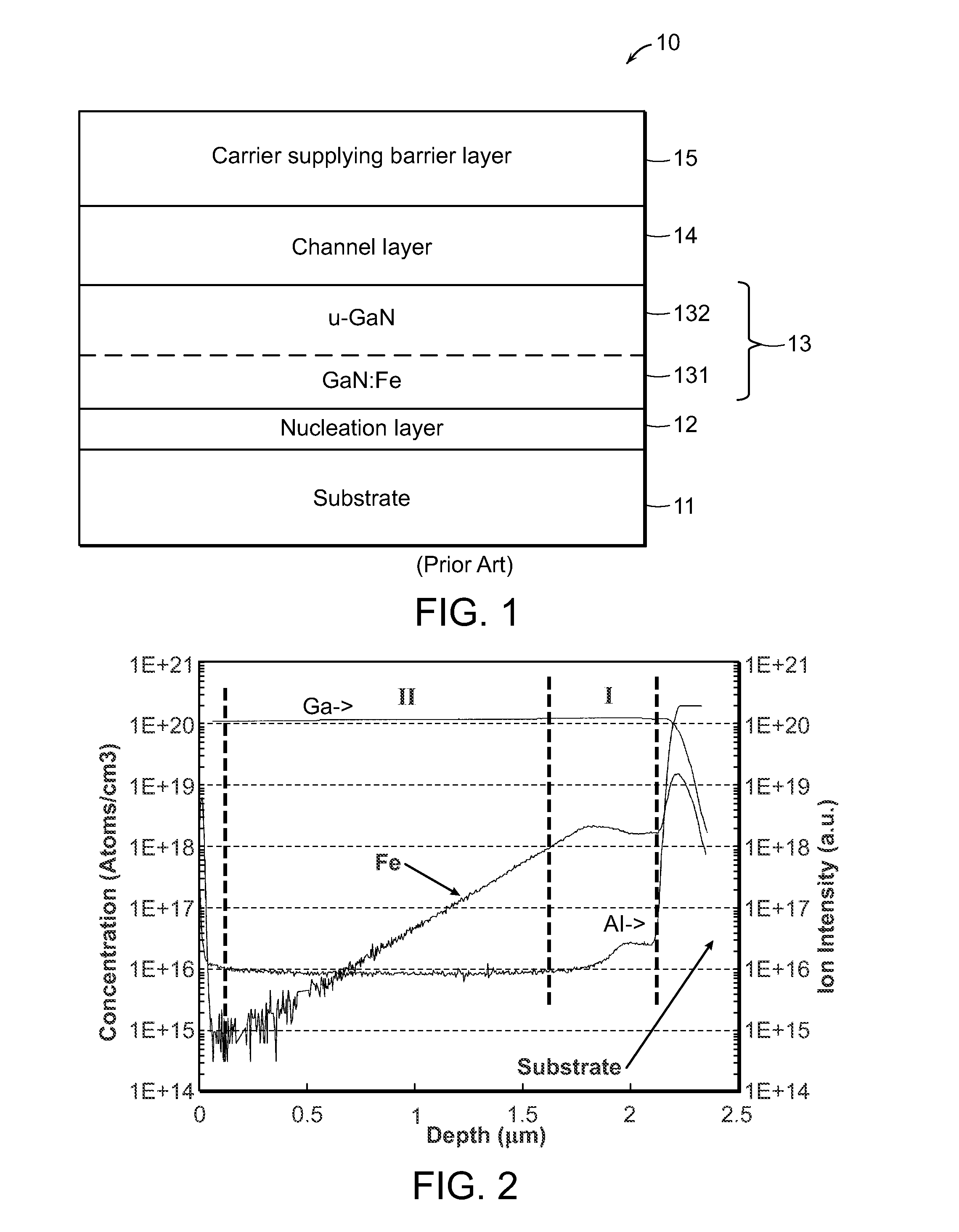
[0016]One embodiment of a prior art high electron-mobility transistor (HEMT) structure is shown in FIG. 1. As represented therein, prior art HEMT structure 10 includes modulated (MD) Fe-doped gallium nitride (GaN) buffer layer 131. HEMT structure 10 includes substrate 11, nucleation layer 12 grown over substrate 11, GaN buffer layer 13 grown over nucleation layer 12 opposite substrate 11, gallium nitride (GaN) channel layer 14 grown over GaN buffer layer 13 opposite nucleation layer 12, and carrier-supplying layer 15 grown over channel layer 14 opposite GaN buffer layer 13. GaN buffer layer 13 includes lower component 131 adjacent to nucleation layer 12 where, during formation, GaN that is deposited on layer 12 is doped with iron (Fe). Upper componen...


PUM


Abstract

An iron-doped high-electron-mobility transistor (HEMT) structure includes a substrate, a nucleation layer over the substrate, and a buffer layer over the nucleation layer. The gallium-nitride buffer layer includes a iron-doping-stop layer having a concentration of iron that drops from a juncture with an iron-doped component of the buffer layer over a thickness that is relatively small compared to that of the iron-doped component. The iron-doping-stop layer is formed at lower temperature compared to the temperature at which the iron-doped component is formed. The iron-doped HEMT structure also includes a channel layer over the buffer layer. A carrier-supplying barrier layer is formed over the channel layer.

Description

BACKGROUND OF THE INVENTION[0001]III-nitride semiconductors are very promising materials for use in high-electron mobility transistor (HEMT) structures, which typically include a carrier-supplying layer and a channel layer supporting the carrier-supplying layer. A semi-insulating buffer layer generally is required for electrical insulation of the HEMT structure from a substrate, and to provide tight charge control of the HEMT channel layer of the HEMT structure. Often, two types of gallium nitride (GaN) buffer layers are employed as the buffer layer: the first being a nominally-undoped GaN layer adjacent to the channel layer where intrinsic defects, such as dislocations and carbon impurity render semi-insulating properties; and the second being a GaN layer relatively remote from the channel layer that is intentionally doped with iron (Fe). The iron-doped buffer layer effectively isolates the HEMT structure from the underlying substrate by trapping free electrons in iron-impurity-rel...

Claims


Application Information

Patent Timeline
IPC IPC(8): H01L29/778H01L29/66
CPCH01L29/66462H01L29/7783H01L29/2003H01L29/36H01L29/7786H01L29/207
Inventor LABOUTIN, OLEGCAO, YUJOHNSON, WAYNE
Owner IQE KC
Why Eureka
Try Eureka