Check patentability & draft patents in minutes with Patsnap Eureka AI!

Non-volatile memory (NVM) and high voltage transistor integration

a technology of high-voltage transistors and non-volatile memories, which is applied in the direction of basic electric elements, electrical equipment, semiconductor devices, etc., can solve the problems of difficult manufacturing, reducing the top surface of the semiconductor substrate, and unable to achieve both desirable characteristics

Active Publication Date: 2015-01-01
NXP USA INC
View PDF6 Cites 1 Cited by
  • Summary
  • Abstract
  • Description
  • Claims
  • Application Information

AI Technical Summary

Benefits of technology

The patent text describes a method of integrating non-volatile memories (NVMs) with high voltage transistors in semiconductor structures. The technical effect of this method is to improve the manufacturing process of NVMs by integrating them with logic transistors that use the same power supply voltage. This helps to achieve higher quality gate dielectric for the NVMs and reduces difficulties in manufacturing. The method also includes using a thick oxide layer for the high voltage transistor's gate dielectric, which can improve the performance of the NVMs.

Problems solved by technology

The high voltage transistors typically have a thicker gate dielectric than the vast majority of the logic transistors which can create difficulties in manufacturing.
Achieving both of these desirable characteristics can be difficult to achieve.
Also there is an undesirable effect of having to grow a particularly thick oxide which consumes silicon and thus lowers the top surface of the semiconductor substrate.

Method used


Image

  • Non-volatile memory (NVM) and high voltage transistor integration
  • Non-volatile memory (NVM) and high voltage transistor integration
  • Non-volatile memory (NVM) and high voltage transistor integration

Examples


Embodiment Construction

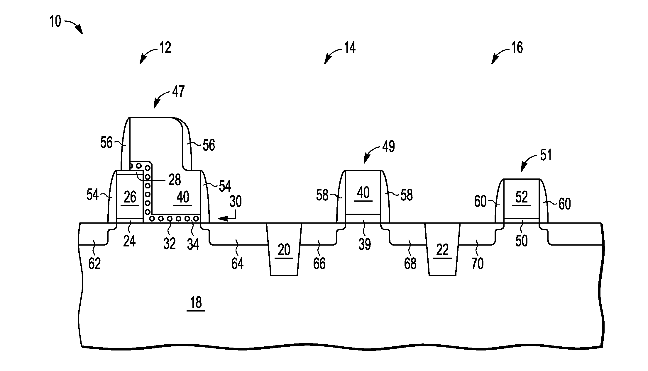
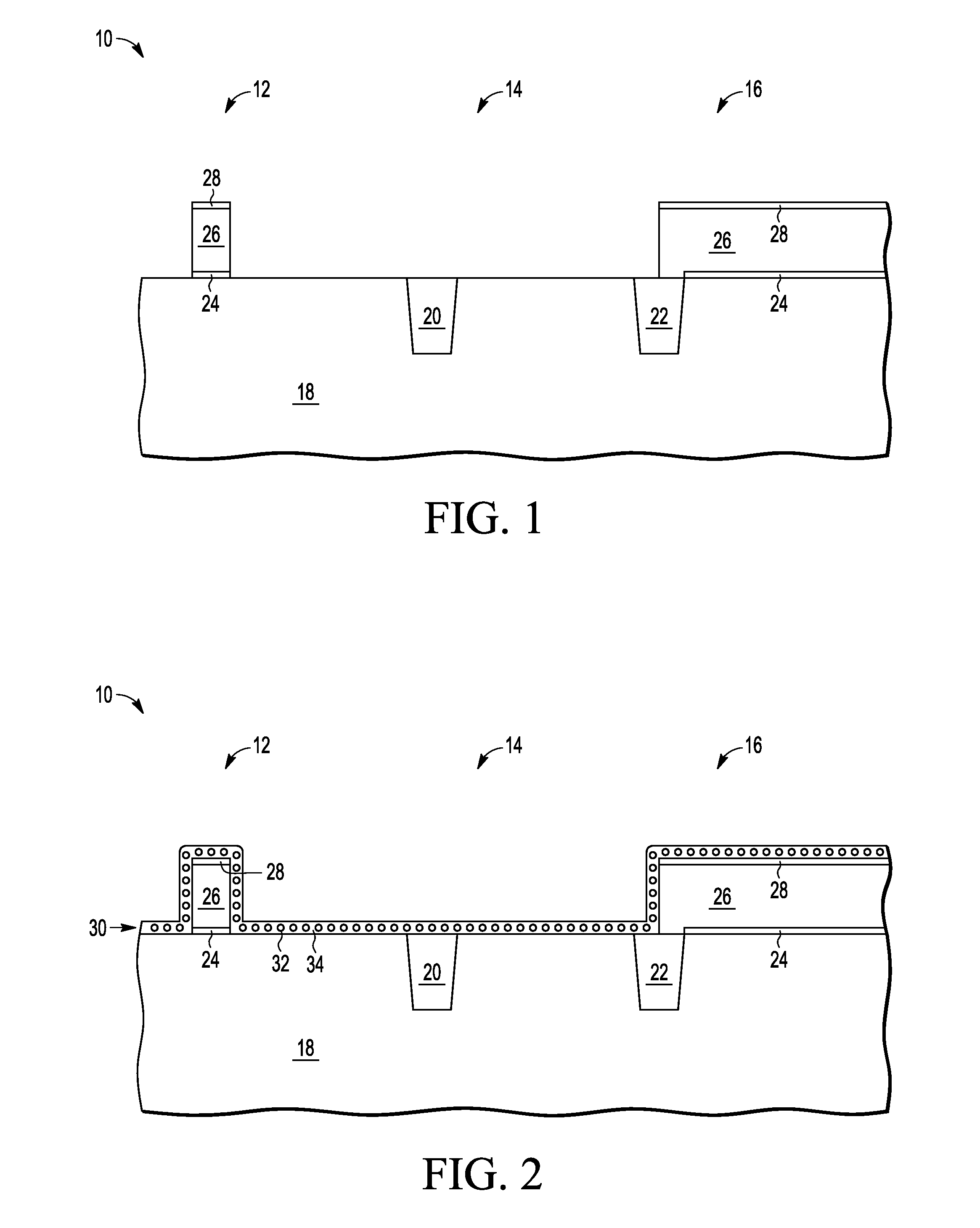
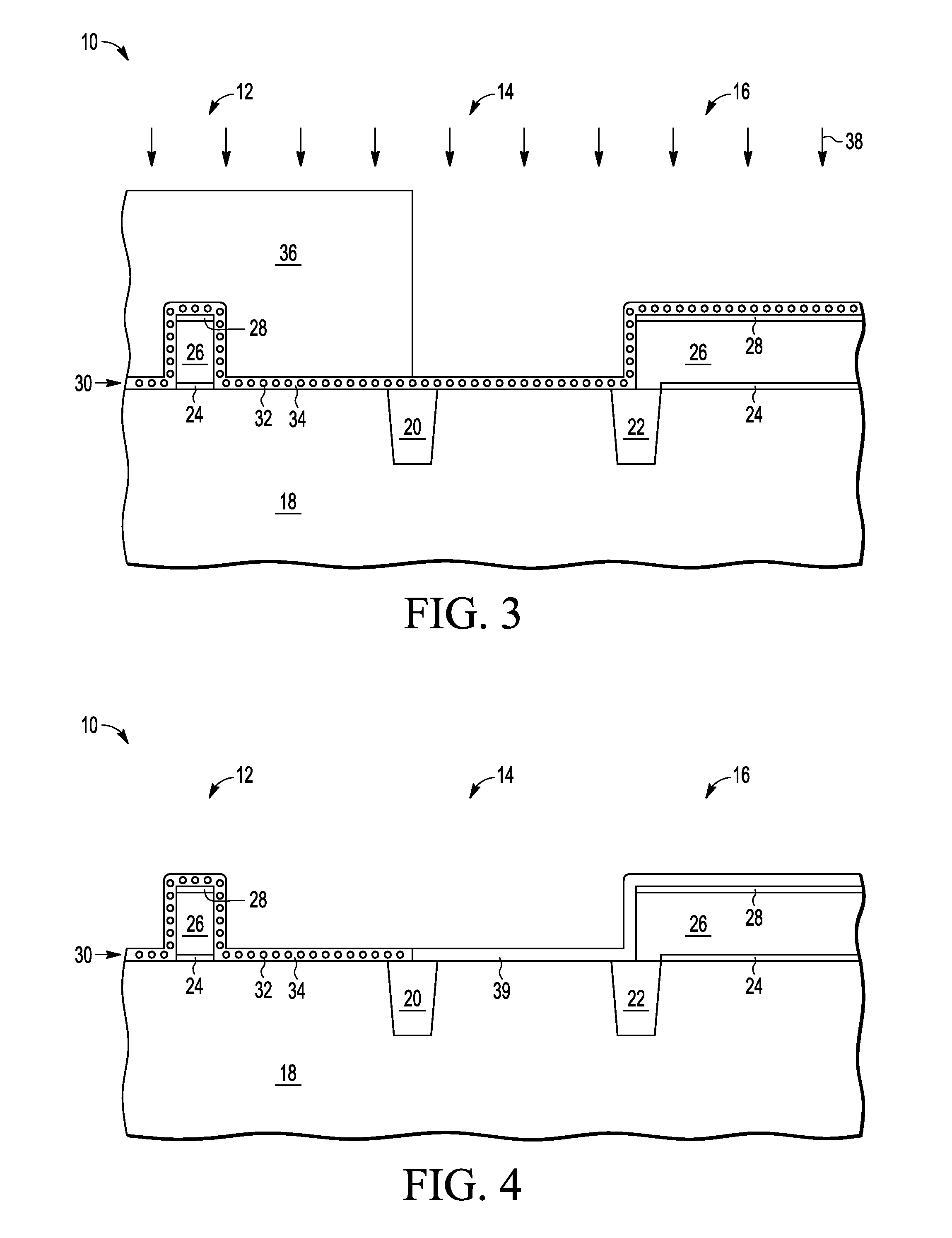
[0022]In one aspect, an integration of a non-volatile memory (NVM) cell and a high voltage transistor includes forming the select gate structure of the NVM cell in the NVM portion and an oxidizable charge storage layer wherein the oxidizable charge storage layer extends to the region of forming the high voltage transistor. The oxidizable charge storage layer is protected for the NVM cell while being oxidized for the high voltage transistor to form a thick oxide layer. The subsequent completion of the high voltage transistor uses the thick oxide for the gate dielectric of the high voltage transistor. This is better understood by reference to the drawings the following the written description.

[0023]The semiconductor substrate described herein can be any semiconductor material or combinations of materials, such as gallium arsenide, silicon germanium, silicon-on-insulator (SOI), silicon, monocrystalline silicon, the like, and combinations of the above. Oxide layer refers to a silicon ox...


PUM


Abstract

A method of making a semiconductor structure includes forming a select gate stack on a substrate. The substrate includes a non-volatile memory (NVM) region and a high voltage region. The select gate stack is formed in the NVM region. A charge storage layer is formed over the NVM region and the high voltage region of the substrate. The charge storage layer includes charge storage material between a bottom layer of dielectric material and a top layer of dielectric material. The charge storage material in the high voltage region is oxidized while the charge storage material in the NVM region remains unoxidized.

Description

BACKGROUND[0001]1. Field[0002]This disclosure relates generally to non-volatile memories (NVMs), and more particularly, integrating NVMs with high voltage transistors.[0003]2. Related Art[0004]The integration of non-volatile memories (NVMs) with high voltage transistors is particularly significant because NVM cells typically use significantly higher voltages for program and erase than the power supply voltage. Most of the transistors generally operate at the power supply voltage and are manufactured with that voltage in mind. The generation and use of the higher voltages required for program and erase require transistors that can operate at those higher voltages. Also, it is common for there to be a need for some ability to handle higher voltages than are used by most of the logic transistors, especially at inputs which can be from higher voltage products such as batteries and even USB inputs. This is often a situation of an analog to digital conversion. The high voltage transistors...

Claims


Application Information

Patent Timeline
IPC IPC(8): H01L29/66H01L29/792
CPCH01L29/66833H01L29/792H01L29/42328H01L29/7881H01L29/66825H01L27/11529H01L27/11546H10B41/41H10B41/49
Inventor HONG, CHEONG MINKANG, SUNG-TAEGYATER, JANE A.
Owner NXP USA INC
Features
  • R&D
  • Intellectual Property
  • Life Sciences
  • Materials
  • Tech Scout
  • Unparalleled Data Quality
  • Higher Quality Content
  • 60% Fewer Hallucinations
Learn More