Finfet-based boosting supply voltage circuit and method

a supply voltage circuit and circuit technology, applied in the field of electrical, electronic and computer arts, can solve the problems of increasing the complexity or overhead of the circuit, increasing the area of the integrated circuit (ic), etc., and achieves the reduction of circuit complexity and overhead, improving performance, and increasing the operating voltage range of the circuit.

Inactive Publication Date: 2015-01-01
IBM CORP
View PDF9 Cites 8 Cited by
  • Summary
  • Abstract
  • Description
  • Claims
  • Application Information

AI Technical Summary

Benefits of technology

[0005]Principles of the invention provide a boosted voltage supply circuit architecture suitable for use, for example, in a memory system or logic circuit, having improved performance and / or reduced circuit complexity and overhead. More particularly, embodiments of the invention provide a dynamic voltage supply boosting technique which beneficially increases the operating voltage range of the circuitry in which the voltage supply boosting technique is used by enabling the circuitry to operate at a lower minimum supply voltage (Vmin). Techniques according to the invention advantageously eliminate the need for multiple voltage supplies in the system while reducing power consumption. In this manner, embodiments of the invention are well-suited for use in low-power applications.

Problems solved by technology

Unfortunately, however, each of the above-noted techniques for improving the stability of 6T or 8T SRAM cells results in one or more disadvantages, such as, for example, increased integrated circuit (IC) area, increased power consumption, increased circuit complexity or overhead, and supply voltage penalty.
However, the use of multiple voltage supplies and their conversion from on-chip is complex, and conversion efficiency is often an issue.
Accordingly, conventional solutions for improving the stability of 6T and 8T SRAM cells are generally not well-suited for low-power applications.
Furthermore, it is difficult to achieve a simplified solution which meets stability, performance and minimum supply voltage (Vmin) requirements of modern applications and systems.

Method used


Image

  • Finfet-based boosting supply voltage circuit and method
  • Finfet-based boosting supply voltage circuit and method
  • Finfet-based boosting supply voltage circuit and method

Examples


Embodiment Construction

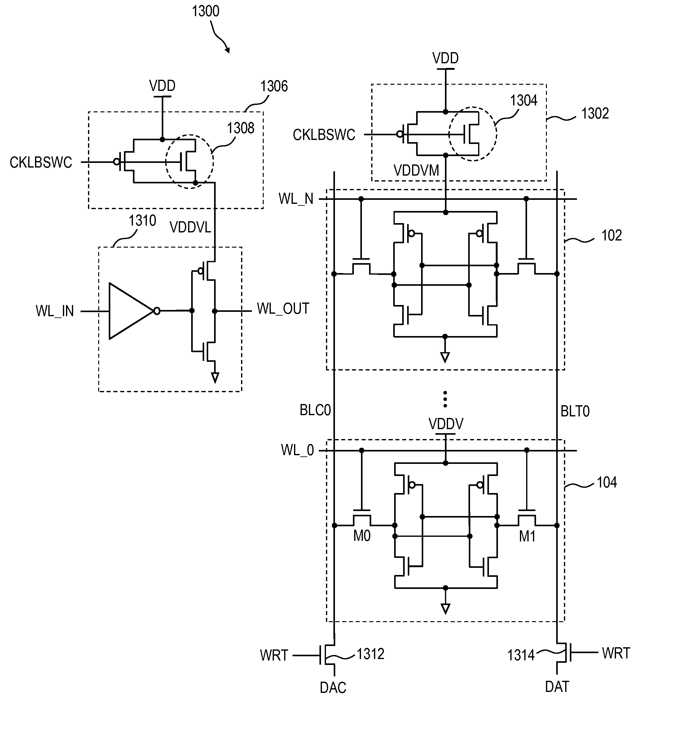
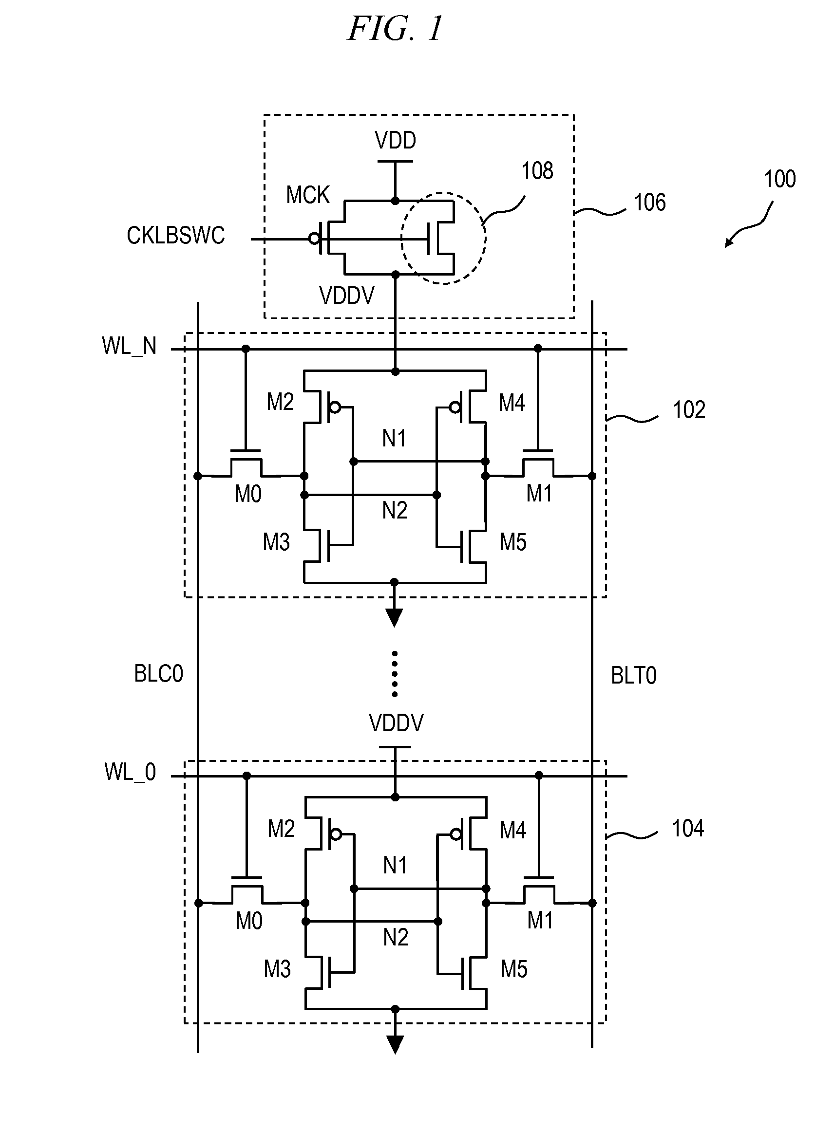
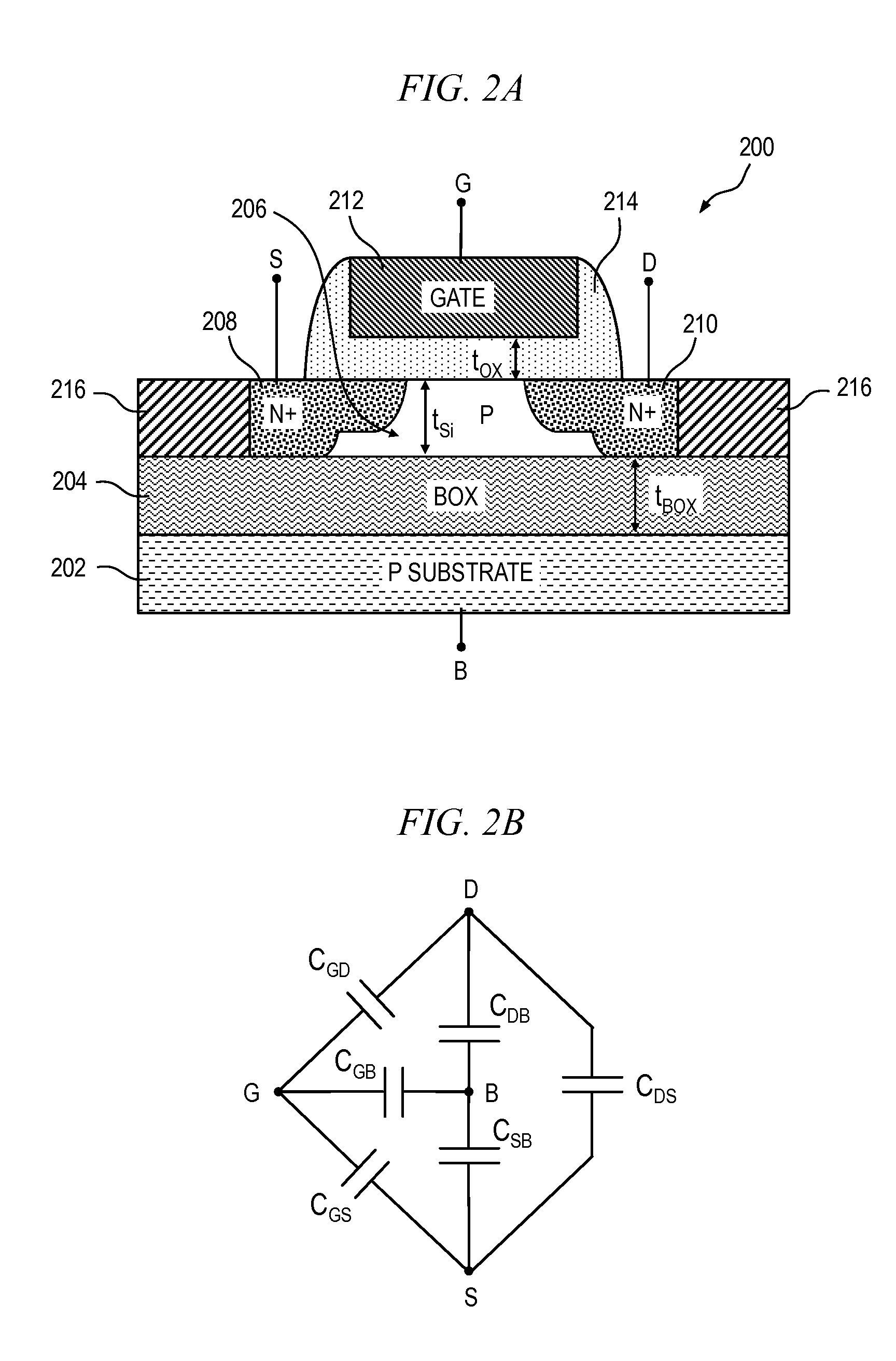
[0023]Principles of the present invention will be described herein in the context of illustrative embodiments of a memory architecture (e.g., employing 6T or 8T SRAM cells) and logic circuitry employing dynamic voltage supply boosting. It is to be appreciated, however, that the invention is not limited to the specific circuits and / or methods illustratively shown and described herein. Rather, aspects of the invention are directed more broadly to techniques for reducing a minimum supply voltage (Vmin) of a circuit, thereby increasing an operational supply voltage range of the circuit. Voltage supply boosting circuitry formed in accordance with embodiments of the invention provide improved performance, particularly a reduced minimum operational supply voltage, without a need for multiple voltage supplies, and are thus well-suited for use in low power applications. Moreover, it will become apparent to those skilled in the art given the teachings herein that numerous modifications can be...


PUM


Abstract

A memory circuit includes a voltage boosting circuit for generating a voltage that exceeds a voltage supply of the voltage boosting circuit. The voltage boosting circuit includes a first transistor having a first polarity type and a second transistor having a second polarity type opposite the first transistor. The first transistor is a planar transistor, a source of the first transistor being connected with the voltage supply, and a gate of the first transistor receiving a control signal. The second transistor includes a gate formed in at least two planes. A source of the second transistor is connected with the voltage supply, a gate of the second transistor receives the control signal, and a drain of the second transistor is connected with a drain of the first transistor and forms an output of the voltage boosting circuit for generating a boosted supply voltage as a function of the control signal.

Description

CROSS-REFERENCE TO RELATED APPLICATIONS[0001]The present application is a continuation of U.S. patent application Ser. No. 13 / 932,153, filed on Jul. 1, 2013, the contents of which are expressly incorporated herein by reference in its entirety for all purposes.BACKGROUND[0002]The present invention relates generally to electrical, electronic and computer arts, and more particularly relates to memory storage components and systems.[0003]In a memory system employing six-transistor (6T) or eight-transistor (8T) static random access memory (SRAM) cells, in order to improve the stability of conventional 6T or 8T memory cells, a variety of techniques have been proposed. Such techniques include, for example, providing dual-voltage supplies, using multiple-threshold voltage (multi-VT) transistor devices, decreasing the length of bit lines used in the memory cells, employing power supply boosting via interconnects, adding transistors to the cells, and using a charge pump to boost the voltage s...

Claims


Application Information

Patent Timeline
Patent Type & Authority Applications(United States)
IPC IPC(8): G11C5/14G11C11/419
CPCG11C5/14G11C11/419G11C5/145G11C11/417
Inventor JOSHI, RAJIV V.KIM, KEUNWOO
Owner IBM CORP
Why Eureka
Try Eureka