Mtj memory cell with protection sleeve and method for making same

Inactive Publication Date: 2015-01-15
AVALANCHE TECH
View PDF3 Cites 19 Cited by
  • Summary
  • Abstract
  • Description
  • Claims
  • Application Information

AI Technical Summary

Benefits of technology

[0006]Embodiments of the invention include methods and structures to reduce metallic redeposition material in memory cells, such as MTJ cells, during pillar etching and thereby reduce or eliminate redeposition material on the MTJ barrier layer sidewall. A first embodiment forms metal studs on top of the MTJ landing pads in a dielectric layer that otherwise covers the exposed metal surfaces on the wafer to prevent exposing the metal to the MTJ etching ambient. The metal studs provide the electrical connection between the bottom electrodes and the landing pads. An optional process for this embodiment adds a touch-up metal layer and a light CMP to ensure a smooth surface for patterning the pillars.
[0007]The second embodiment patterns the MTJ and bottom electrode separately. The bottom electrode mask then covers metal under the bottom electrode. In this embodiment the MTJ mask can be patterned before or after the bottom electrode mask. The embodiment where the bottom electrode is defined prior to the MTJ includes depositing a dielectric layer used to stop bottom electrode etching to prevent building a deep step structure at the edge of the bottom electrode. This avoids the problem of the MTJ stack deposited on sidewall of the deep

Problems solved by technology

Once the etching process that forms the pillars passes through the barrier layer, the exposed

Method used


Image

  • Mtj memory cell with protection sleeve and method for making same
  • Mtj memory cell with protection sleeve and method for making same
  • Mtj memory cell with protection sleeve and method for making same

Examples


first embodiment

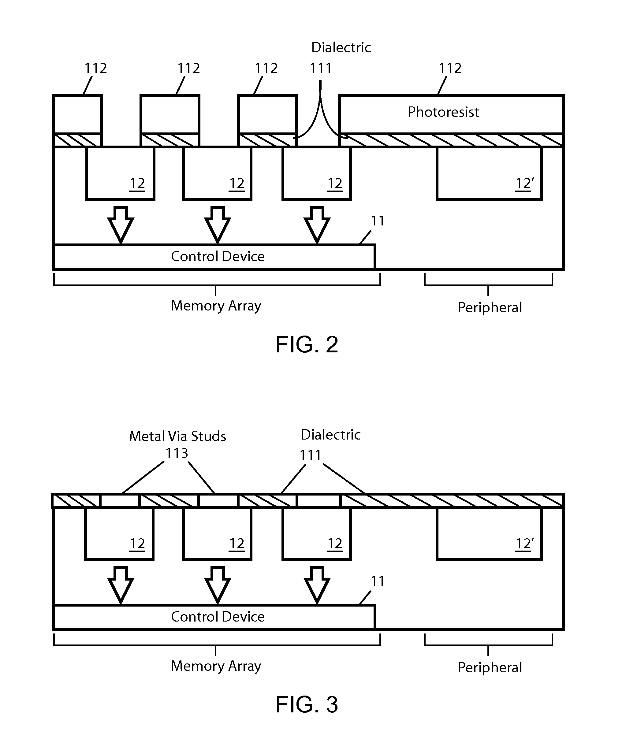
[0025]FIG. 2-FIG. 5 illustrate cross sectional views of selected process stages for the first embodiment which minimizing exposure of landing pad metal by MTJ over-etching. As shown in FIG. 2, after the landing pad patterning process has been completed, a dielectric layer 111 is first deposited over the wafer on the exposed landing pads 12, 12′. Next using a conventional lithography process, photoresist mask 112 has been deposited and patterned as shown to allow the dielectric material to be dry etched away from the center area of the tops of the landing pads 12 while peripheral landing pad 12′ remain protected. The photoresist mask 112 covers the peripheral area metal during this etching. The gaps in the mask over the landing pads are smaller in horizontal area than the upper surface of the landing pad. This allows dielectric material to remain on the outer edges of the landing pads 12 after etching, but central vias have been formed exposing a portion of the upper surface of the l...

second embodiment

[0029]The second embodiment patterns the MTJ and bottom electrode separately. An etch-stop layer is deposited on the ILD before the landing pads are formed by the damascene process. In this embodiment the MTJ mask can optionally be patterned before or after the bottom electrode mask. In one alternative the bottom electrode mask covers metal under the bottom electrode. The embodiment where the bottom electrode is defined prior to MTJ, the etch-stop layer stops bottom electrode etching to prevent building a deep step structure at the edge of the bottom electrode. This avoids the problem of the MTJ stack deposited on sidewall of the deep step being difficult to clean away.

[0030]FIG. 6-FIG. 11 illustrate cross sectional views of selected process stages for the second embodiment which cover the landing pads 12 and peripheral pad 12′ with an additional bottom electrode mask that is separate from an MTJ mask. Etch-stop layer structures 121 for the bottom electrode etching are patterned on ...

third embodiment

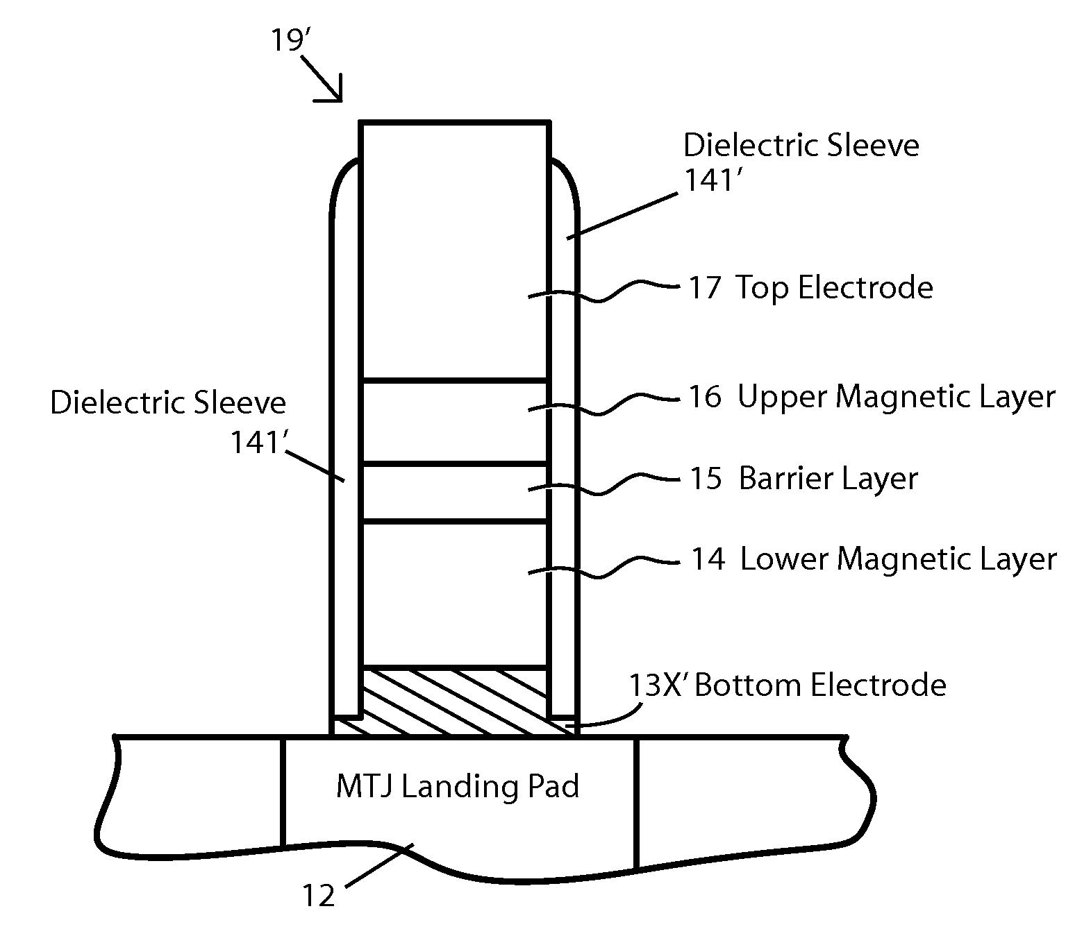
[0036]FIG. 11-FIG. 14 illustrate cross sectional views of selected process stages for the third embodiment. The set of layers for the MTJ device, including a hard mask above the top electrode, is first deposited in sequence. Each of these layers including the hard mask can be standard materials. The photoresist (not shown) for the pillars is patterned by using conventional lithography and then dry etching proceeds to achieve the stage as shown in FIG. 11, where the etching process has been stopped as soon the barrier layer has been etched through or optionally at any point in the barrier layer. At this stage partially formed pillars 19B include the barrier layer and all layers above it. The layers for the lower magnetic layer 114 and the bottom electrode 113 are still continuous full films. The top layer of pillars 19B is the hard mask (not shown).

[0037]A subsequent stage is illustrated in FIG. 12 after an oxygen free dielectric material has deposited without breaking vacuum and the...


PUM


Abstract

Methods and structures are described to reduce metallic redeposition material in the memory cells, such as MTJ cells, during pillar etching. One embodiment of the present invention as applied to a memory cell comprises a top electrode layer, an upper magnetic layer, a barrier layer, a lower magnetic layer and a bottom electrode layer in a pillar formed on a landing pad; and a sleeve of dielectric material generally surrounding sidewalls of at least the barrier layer and the lower magnetic layer and partially surrounding the bottom electrode layer. The bottom electrode layer includes a ledge that extends under the sleeve of dielectric material and separates the sleeve of dielectric material from the landing pad under the bottom electrode layer.

Description

RELATED APPLICATION[0001]The present application is a continuation-in-part of the commonly assigned application bearing Ser. No. 13 / 530,381 filed Jun. 22, 2012, entitled “Redeposition Control in MRAM Fabrication Process,” which is incorporated herein by reference.FIELD OF THE INVENTION[0002]The present invention relates generally to semiconductor Back-End-Of-Line (BEOL) memories and particularly to Magnetic Random Access Memory (MRAM) and particularly to techniques and structures for preventing metallic redeposition on sidewalls of the memory element during fabrication.BACKGROUND[0003]The BEOL memories such as RRAM (Resistive Random Access Memory), PRAM (Phase Change Random Access Memory), and MRAM have a resistive device as a memory element. Because high speed access and non-volatility at power off are promised by these devices, they may replace existing memories and create new markets.[0004]FIG. 1B illustrates a typical in-process MTJ memory device 19 at a selected stage during th...

Claims


Application Information

Patent Timeline
IPC IPC(8): H01L43/02G11C11/16H01L43/12G11C11/15
CPCH01L43/02G11C11/161G11C11/15H01L43/12H10B61/10H10B61/22H10N50/80H10N50/01
Inventor SATOH, KIMIHIROJUNG, DONG HAKESHTBOD, PARVIZABEDIFARD, EBRAHIMHUAI, YIMINGZHANG, JING
Owner AVALANCHE TECH
Why Eureka
Try Eureka