Barrier materials for display devices
a technology of barrier materials and display devices, applied in the direction of coatings, transistors, chemical vapor deposition coatings, etc., can solve the problems of current leakage or other types of device failure, material temperature processing limitation of about 350° c. or less, and material failure of other types of devices
- Summary
- Abstract
- Description
- Claims
- Application Information
AI Technical Summary
Benefits of technology
Problems solved by technology
Method used
Image

Examples
example 1
Deposition of Silicon-Containing Films Using Trisilylamine (TSA) and Ammonia (NH3)
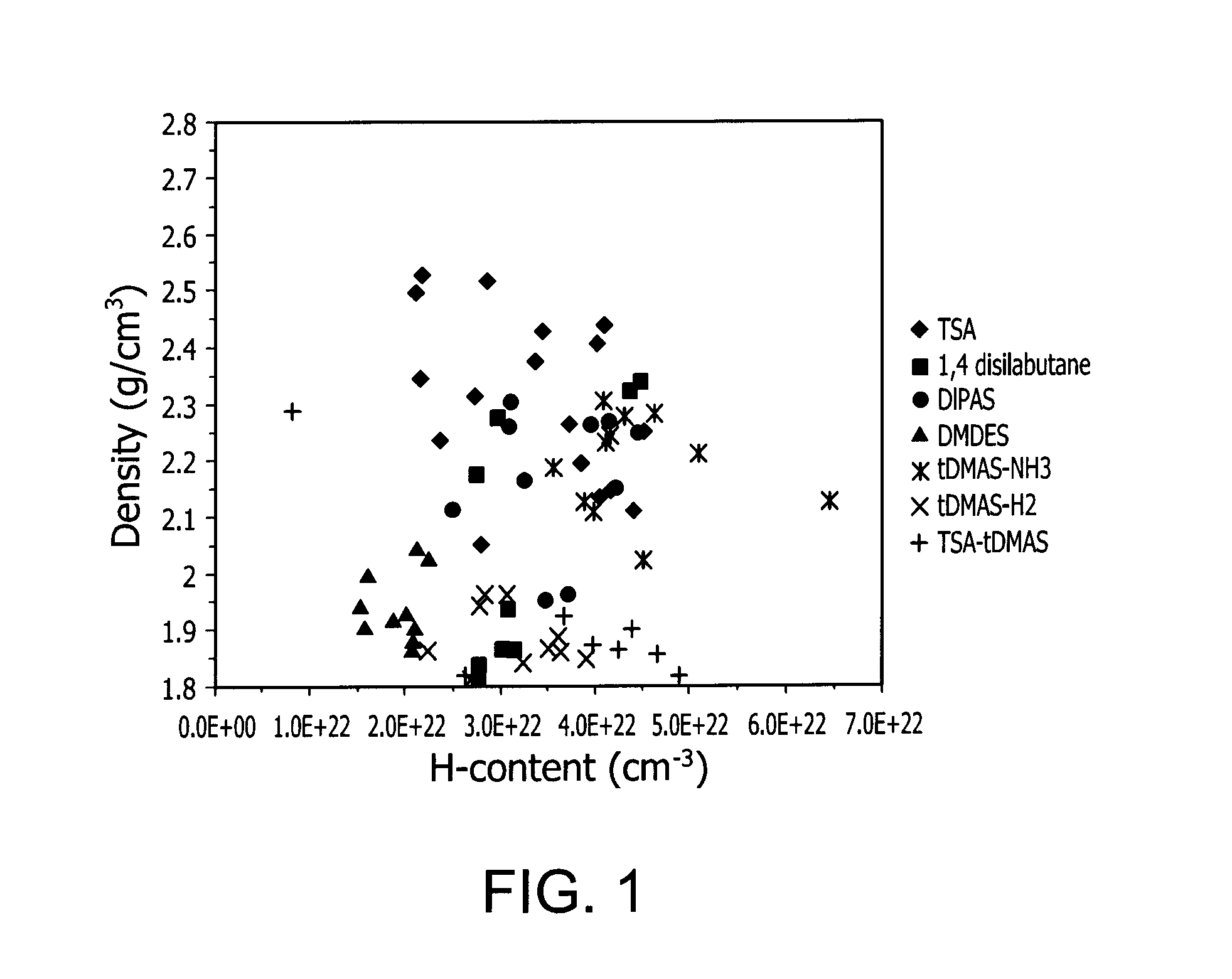
[0095]A number of silicon-containing films were deposited using trisylamine (USA) as precursor onto a 8 inch silicon substrate to see if any of the films would be suitable passivation layers in terms of density and hydrogen content. The composition of the films were measured by XPS and RBS / HFS and showed that the films were comprised of SixNy:Hz wherein the amount of silicon, nitrogen, and hydrogen or x, y, and z varied in atomic percentage depending upon the film. FIG. 1 shows the density versus H-content relationship for these barrier films deposited using TSA precursor.
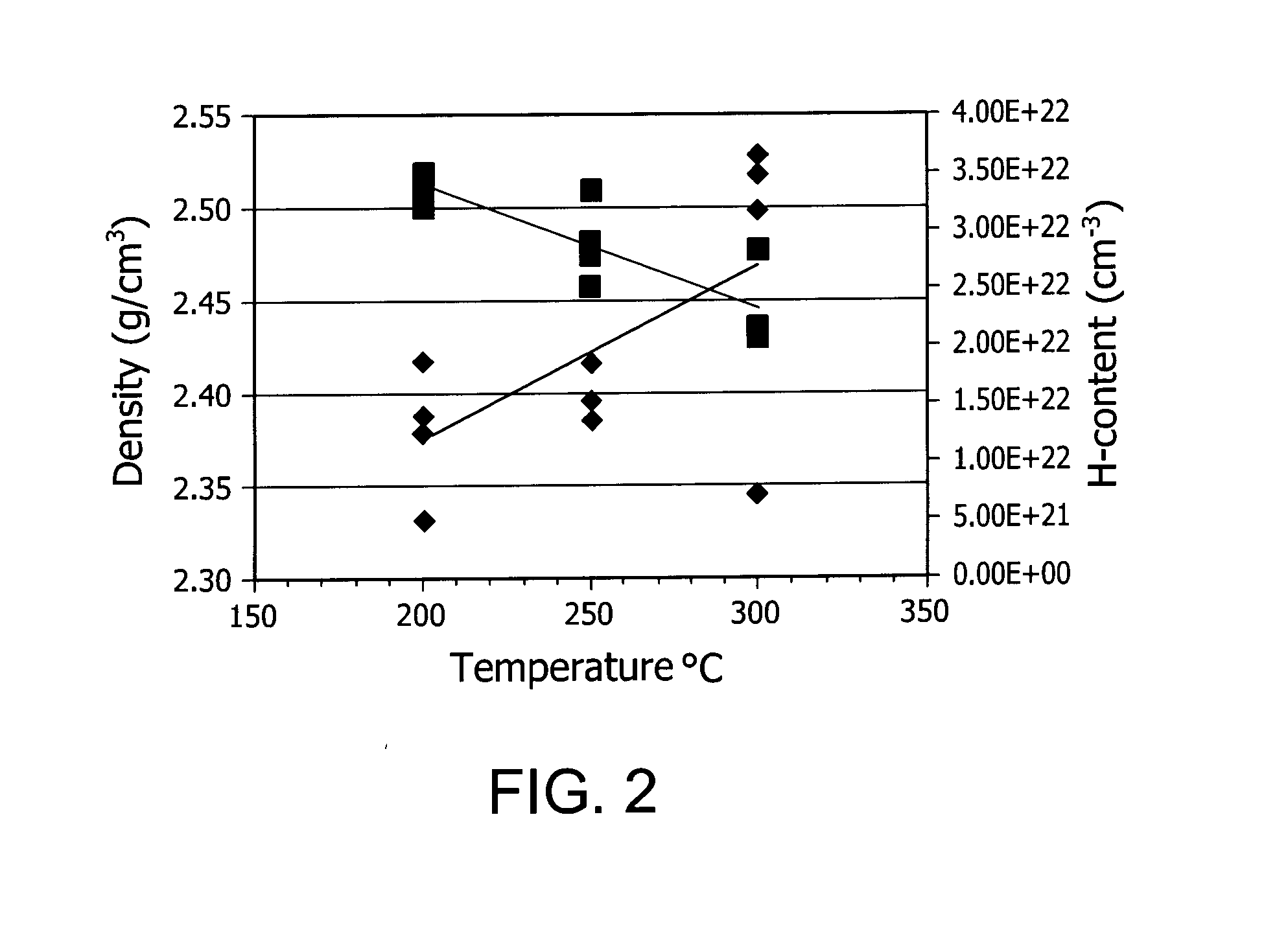
[0096]Of the films deposited by TSA and shown in FIG. 1, the process conditions used to deposit the silicon-containing films having the highest density and lowest hydrogen content using TSA were as follows TSA flow (100-200 mgm), NH3 flow (100 sccm), He (1000 sccm), Pressure (2 torr), RF (400 W), LF (0-100 W), and Temp (300° C.). Of t...
example 8
Comparison of Moisture Barrier Performance for Silicon Containing Layers Deposited Using TEOS and TSA Passivation Layers
[0109]In order to evaluate the relative moisture barrier performance of the silicon-containing films deposited in the above examples, a test was developed to measure this property. In this test, a less dense silicon dioxide (SiO2) layer is first deposited using TEOS at 250° C. onto a silicon wafer under process conditions which render the film sensitive to moisture. When such films are exposed to atmospheric moisture, or alternatively for this comparative test an accelerated test which uses an atmosphere of 85% humidity at 85° C., the film stress changes from tensile to compressive. In this example and in FIG. 6, the dense TEOS and dense TSA films were compared to evaluate their relative moisture barrier performance. Both films were deposited on the less dense TEOS oxide film.
[0110]To measure barrier performance, a thin layer of an exemplary silicon-containing film...
example 9
Evaluation of the Effect of Thickness of PECVD Silicon Oxide Atop In—Ga—Zn—O (IGZO) Metal Oxide Film Wherein Silicon Oxide Layer Further Topped with Silicon
Nitride Layer
[0112]FIG. 6 provides an exemplary structure of a display device comprising a IGZO metal oxide layer 610, a plasma-enhanced chemical vapor deposition (PECVD) silicon oxide layer 630 deposited by tetraethoxysilane (TEOS), and a silicon nitride layer 640 deposited by TSA and NH3 to provide a density silicon nitride a 2.36 g / cm3. The thickness of the silicon oxide layer 630 was varied from 0 to 250 nanometers (e.g., 15 nm, 60 nm, 115 nm, 185 nm, 200 nm, and 250 nm) to determine its impact on minority carrier lifetime. The thickness of the TSA silicon nitride layer was approximately 100 nm. The films were deposited according to the general deposition conditions described above and the following process conditions: (1) TEOS: Power=910 W, Pressure=8.2 Torr, TEOS flow=1000 mg / min, O2 flow=1000 sccm, He flow=1000 sccm; and (...
PUM
| Property | Measurement | Unit |
|---|---|---|
| Temperature | aaaaa | aaaaa |
| Temperature | aaaaa | aaaaa |
| Temperature | aaaaa | aaaaa |
Abstract
Description
Claims
Application Information
 - R&D
- Intellectual Property
- Life Sciences
- Materials
- Tech Scout
- Unparalleled Data Quality
- Higher Quality Content
- 60% Fewer Hallucinations
Browse by: Latest US Patents, China's latest patents, Technical Efficacy Thesaurus, Application Domain, Technology Topic, Popular Technical Reports.
© 2025 PatSnap. All rights reserved.Legal|Privacy policy|Modern Slavery Act Transparency Statement|Sitemap|About US| Contact US: help@patsnap.com