Process for fabrication of spacer layer with reduced hydrogen content in semiconductor device

a technology of semiconductor devices and spacer layers, which is applied in the direction of semiconductor devices, electrical equipment, instruments, etc., can solve the problems of affecting the subthreshold slope or transconductance, the method imparting a significant hydrogen content into silicon nitride, and the degradation of device properties

Active Publication Date: 2005-09-27
MONTEREY RES LLC
View PDF22 Cites 48 Cited by
  • Summary
  • Abstract
  • Description
  • Claims
  • Application Information

AI Technical Summary

Benefits of technology

[0010]The present invention, in one embodiment, relates to a process for fabricating a semiconductor device including steps of providing a semiconductor substrate having formed thereon a semiconductor device; depositing over the semiconductor device a spacer layer, the spacer layer having a first hydrogen content; and applying a treatment to reduce the first hydrogen content to a second hydrogen content.

Problems solved by technology

While the recent advances in charge trapping dielectric flash memory technology have enabled memory designers to double the memory capacity of charge trapping dielectric flash memory arrays using dual-bit data storage, numerous challenges remain in the fabrication of material layers within these devices.
The conventional gate stack spacer is deposited by PECVD, but this method imparts a significant hydrogen content into the silicon nitride.
The present inventors have discovered that hydrogen contained in structures such as the gate stack spacer can migrate into the dielectric layers such as the oxide spacer layer and into the bottom or tunnel oxide layer, and / or into the top oxide layer, and can cause problems such as degradation of device properties.
These problems may include adverse effects on the subthreshold slope or transconductance GM after program / erase as a result of the migration.

Method used


Image

  • Process for fabrication of spacer layer with reduced hydrogen content in semiconductor device
  • Process for fabrication of spacer layer with reduced hydrogen content in semiconductor device
  • Process for fabrication of spacer layer with reduced hydrogen content in semiconductor device

Examples


Embodiment Construction

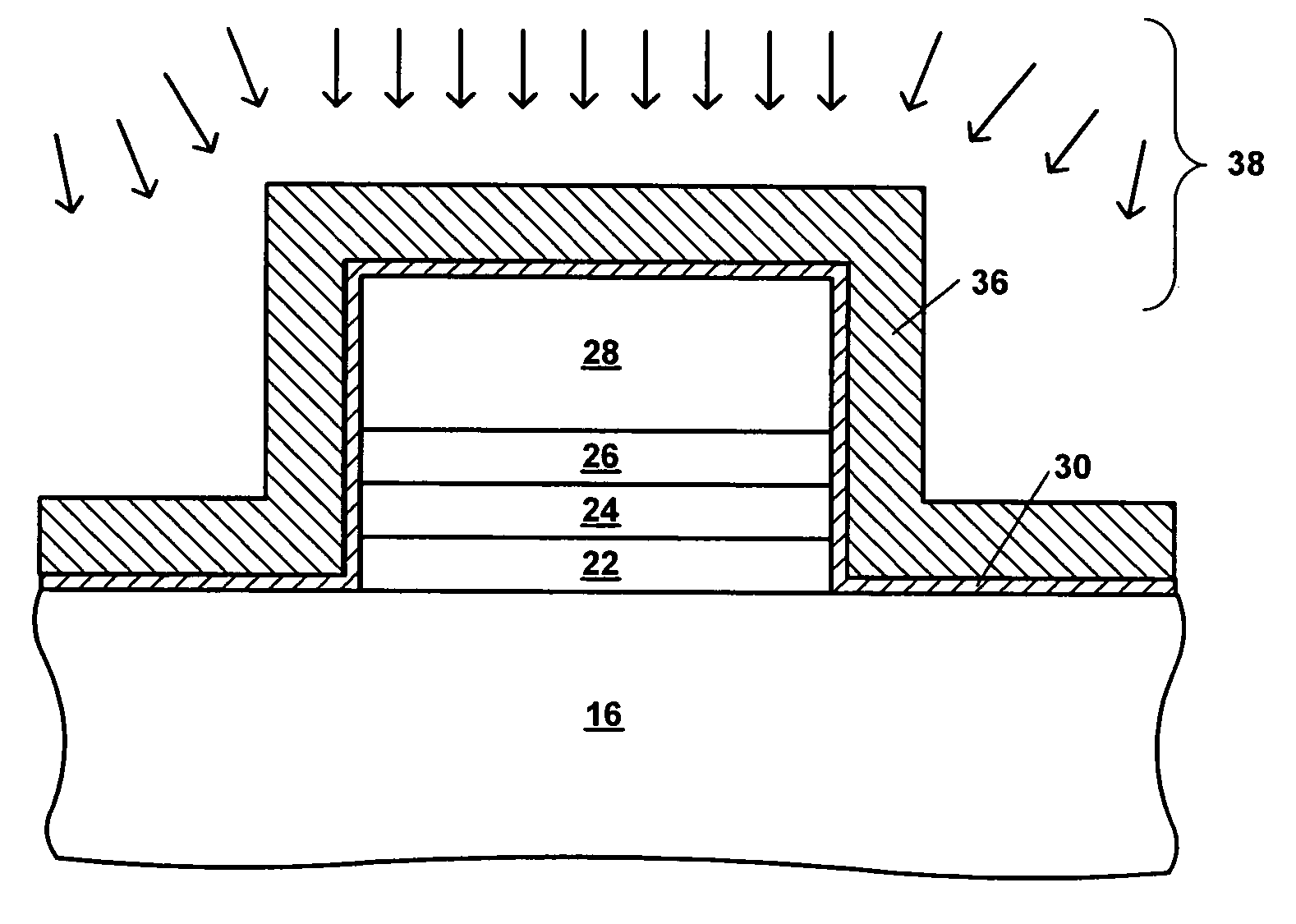
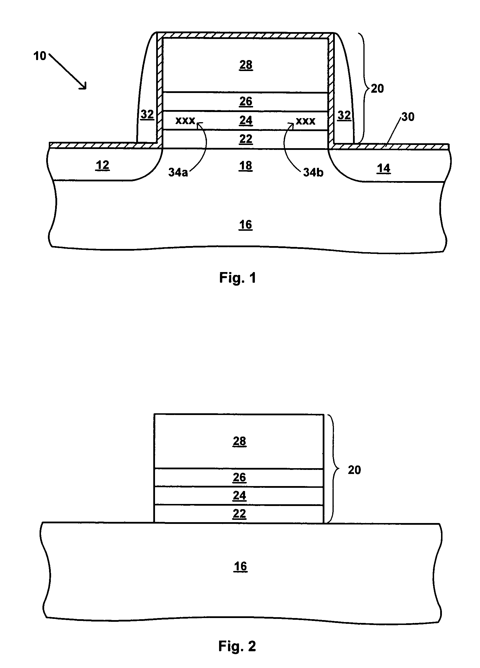
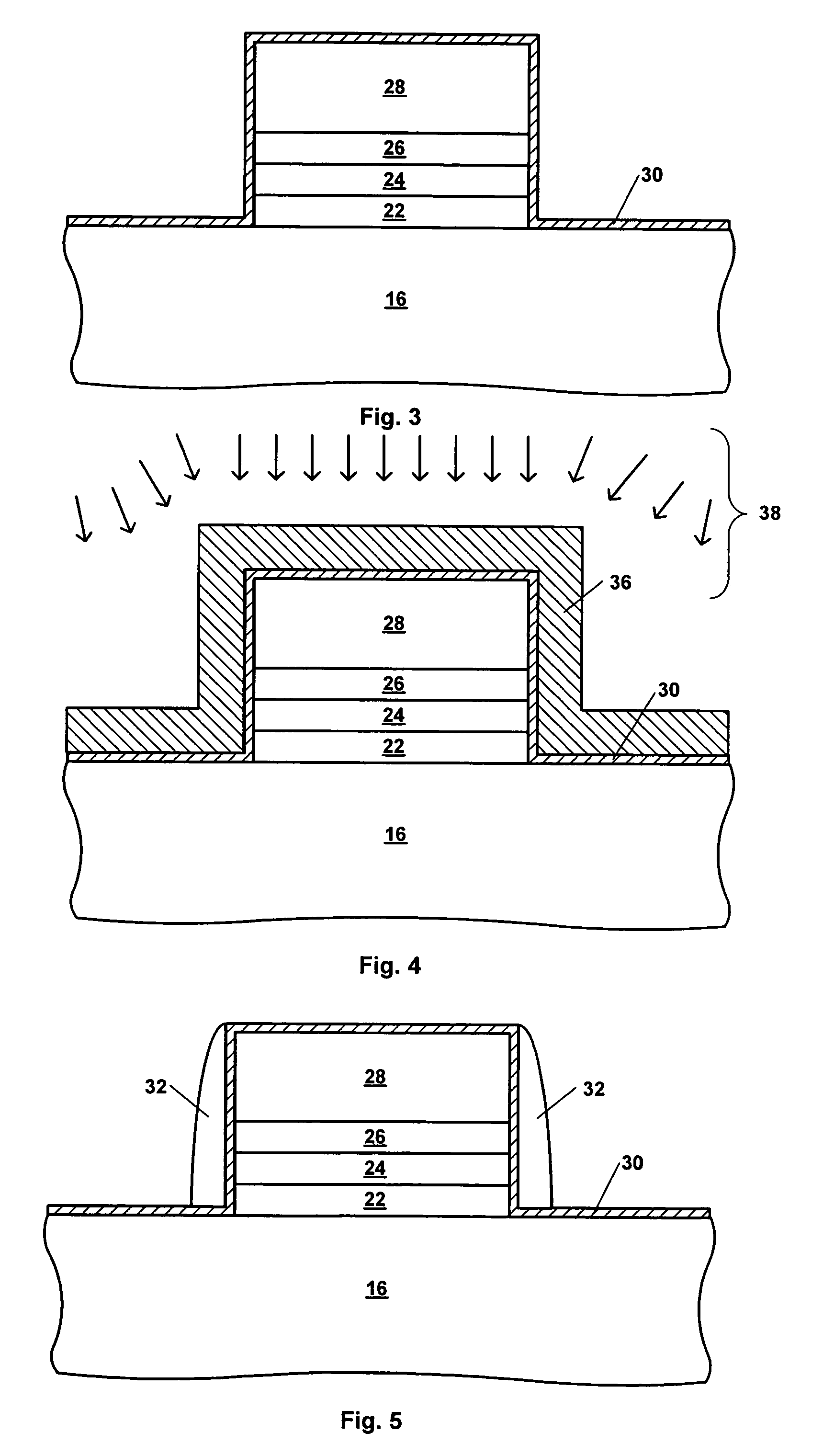
[0020]It should be appreciated that while the present invention will be described in terms of a charge trapping dielectric flash memory device, the present invention is not limited to such device, and is applicable to a broad range of semiconductor devices and their fabrication processes. Generally speaking the semiconductor devices will include at least one active component therein, for example a diode, transistor, thyristor or the like. Illustrative examples include MOS-based devices such as MOSFET devices, including CMOS and NMOS technology, light-emitting diodes, laser diodes, and the like. In this regard, the MOS-based technology discussed herein is intended to encompass the use of gate conductors other than metals as is commonly practiced, and thus reference to MOS-based devices encompasses other insulated gate technologies (e.g. IGFETs). While aspects of the present invention will now be described in more detail with reference to a charge trapping dielectric flash memory devi...


PUM


Abstract

Process for fabricating a semiconductor device including steps of providing a semiconductor substrate having formed thereon a semiconductor device; depositing over the semiconductor device a spacer layer, the spacer layer having a first hydrogen content; and applying a treatment to reduce the first hydrogen content to a second hydrogen content. The invention is particularly useful when applied to flash memory devices such as a charge trapping dielectric flash memory device.

Description

TECHNICAL FIELD[0001]The present invention relates to semiconductor devices and the fabrication thereof and, more particularly, to a charge trapping dielectric flash memory device with reduced hydrogen content in gate stack spacer material and a method of formation of the gate stack spacer with reduced hydrogen content.BACKGROUND ART[0002]Non-volatile memory devices are currently in widespread use in electronic components that require the retention of information when electrical power is terminated. Non-volatile memory devices include read-only-memory (ROM), programmable-read-only memory (PROM), erasable-programmable-read-only memory (EPROM), and electrically-erasable-programmable-read-only-memory (EEPROM) devices. EEPROM devices differ from other non-volatile memory devices in that they can be electrically programmed and erased. Flash EEPROM devices are similar to EEPROM devices in that memory cells can be programmed and erased electrically. However, flash EEPROM devices enable the...

Claims


Application Information

Patent Timeline
Patent Type & Authority Patents(United States)
IPC IPC(8): H01L21/02H01L21/31H01L21/28H01L21/314H01L21/316H01L21/336
CPCG11C16/0475H01L21/0217H01L21/02326H01L21/02337H01L21/0234H01L21/28282H01L21/3105H01L29/6656H01L29/66833H01L29/40117
Inventor HALLIYAL, ARVINDCHEUNG, FRED T KSUGINO, RINJISHIRAIWA, HIDEHIKOKAMAL, TAZRIENYANG, JEAN Y.
Owner MONTEREY RES LLC
Why Eureka
Try Eureka