

Transparent conductive film, conductive element, composition, colored self-assembled material, input device, display device, and electronic instrument
Inactive Publication Date: 2015-02-05
DEXERIALS CORP
View PDF6 Cites 11 Cited by
- Summary
- Abstract
- Description
- Claims
- Application Information
AI Technical Summary
Benefits of technology
The patent describes a technique that prevents light from reflecting too widely on the surface of a metal filler while maintaining the conductivity of the material.
Problems solved by technology
However, transparent conductive films using a metal oxide have been expensive to produce because of sputter deposition under vacuum environment and easy to cause cracking and separation by deformation such as bending and deflection.
However, when a transparent conductive film including a metal filler is provided on the display screen side of a display panel, diffuse reflection of outside light occurs on the surface of the metal filler, so that black display of the display panel slightly becomes bright, which is called a milky appearance (whitish appearance).
Method used
View moreImage
Smart ImageViewing Examples

Examples
embodiments
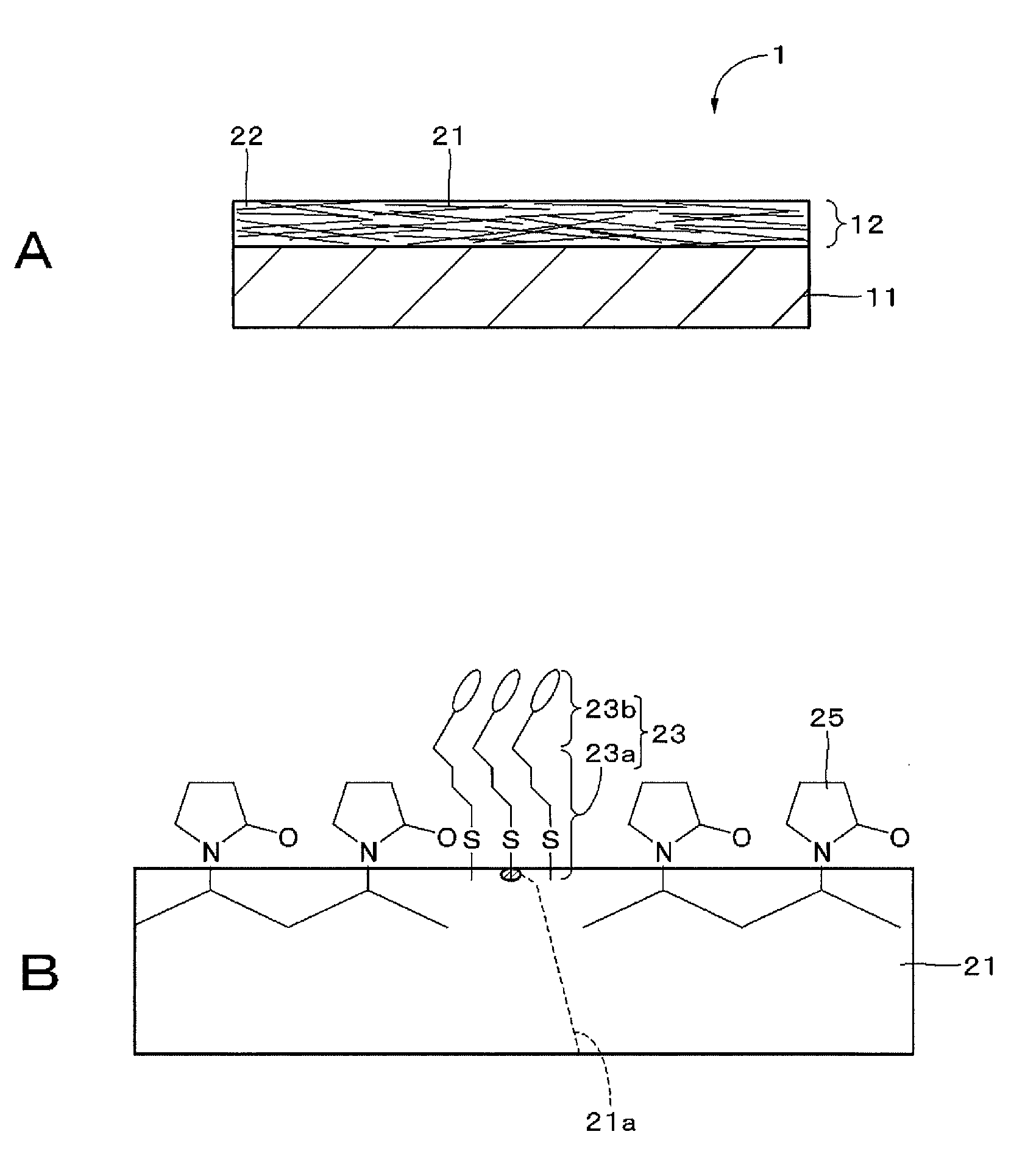
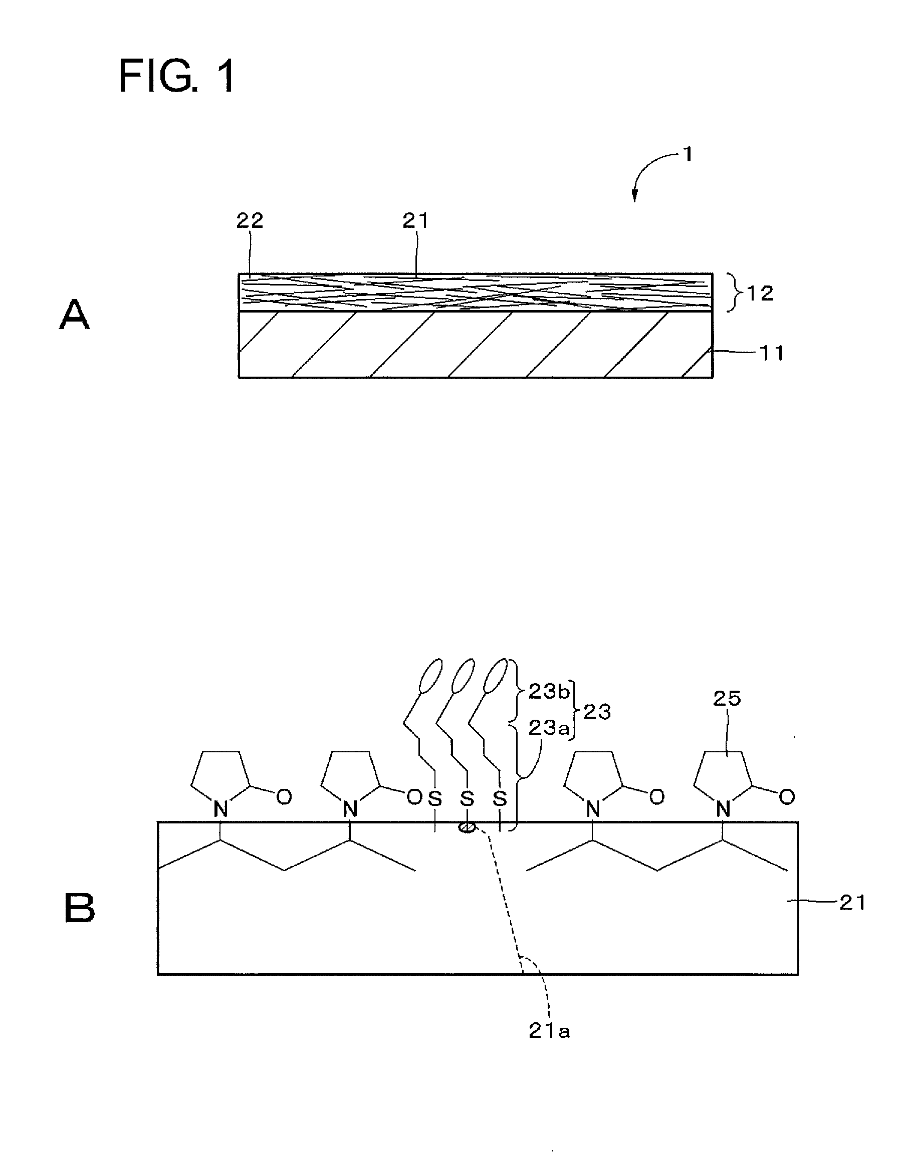
[0073]Embodiments of the present technique will be described in the following order with reference to the drawings:
first embodiment (
1. First embodiment (Example of configuration of transparent conductive element);
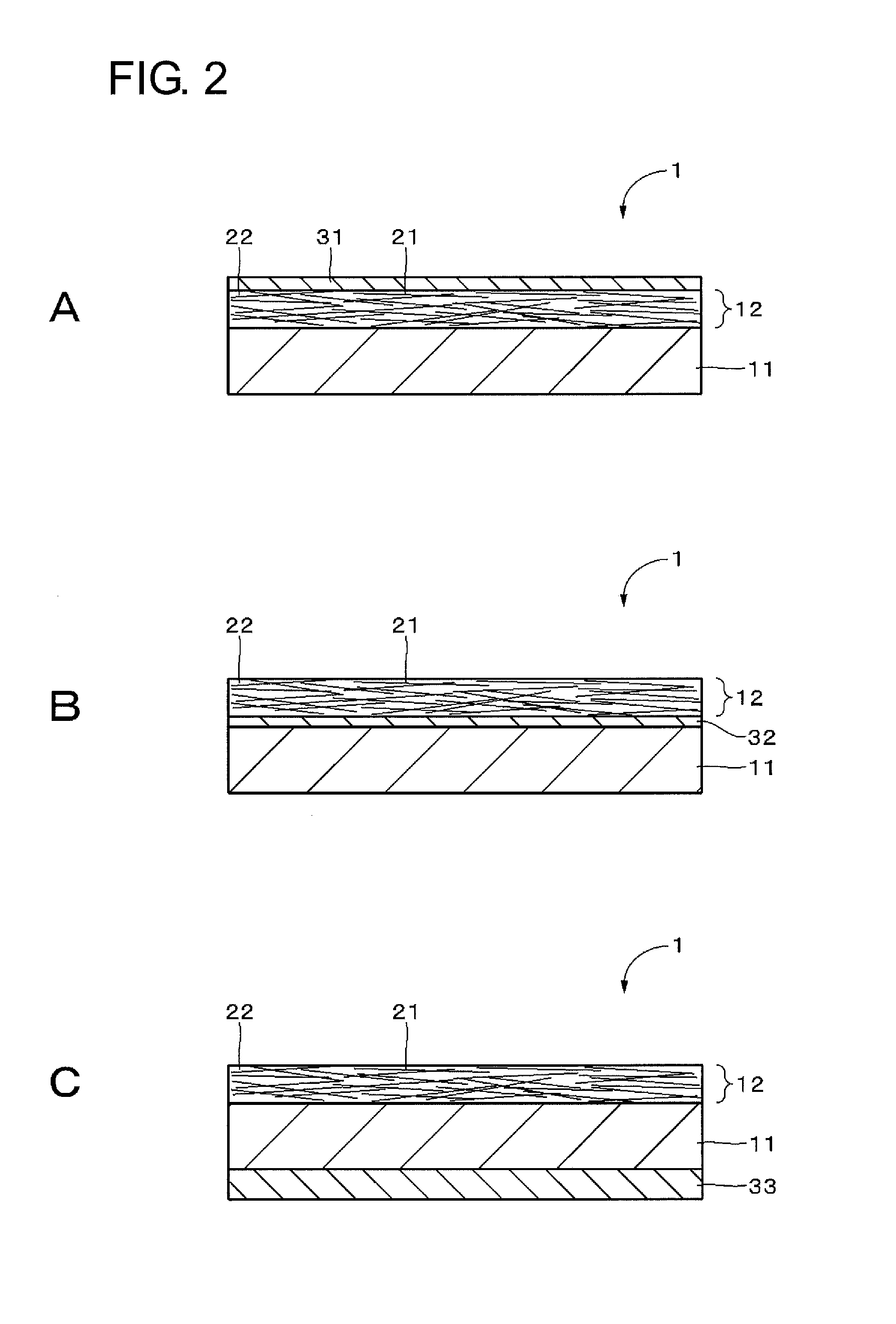
second embodiment (
2. Second embodiment (Example of configuration of transparent conductive element having patterned transparent conductive film);
Login to View More PUM
| Property | Measurement | Unit |
|---|---|---|
| Electrical conductor | aaaaa | aaaaa |
| Transparency | aaaaa | aaaaa |
Abstract
A transparent conductive film includes a metal filler and a colored self-assembled material adsorbed to the surface of the metal filler. This transparent conductive film can prevent diffuse reflection of light on the surface of the metal filler.
Description
TECHNICAL FIELD[0001]The present technique relates to a transparent conductive film, a conductive element, a composition, a colored self-assembled material, an input device, a display device, and an electronic instrument, and more particularly to a transparent conductive film including a metal filler.BACKGROUND ART[0002]Metal oxides such as indium tin oxide (ITO) have been used in transparent conductive films, which require optical transparency, such as transparent conductive films provided on the display screen of a display panel, particularly transparent conductive films of information input devices disposed on the display screen side of a display panel. However, transparent conductive films using a metal oxide have been expensive to produce because of sputter deposition under vacuum environment and easy to cause cracking and separation by deformation such as bending and deflection.[0003]Therefore, transparent conductive films including a metal filler have been studied which can s...
Claims
Login to View More Application Information
Patent Timeline
 IPC IPC(8): G02B1/04G02B5/23G06F1/16
CPCG02B1/04G02B5/23G06F1/1637G06F3/041H01B1/22B32B27/08B32B27/20B32B2264/105B32B2307/202B32B2307/402B32B2307/412B32B2457/20Y10T428/256H10K50/81H10K50/828G06F3/00H01B5/14G06F2203/04103B32B7/025
InventorKANEKO, NAOTOMIZUNO, MIKIHISALEE, SUNG-KILIWATA, RYOSUKEISHII, YASUHISA
OwnerDEXERIALS CORP