
Lead-Free Solder Alloy

Inactive Publication Date: 2015-02-05
SENJU METAL IND CO LTD
View PDF18 Cites 5 Cited by
  • Summary
  • Abstract
  • Description
  • Claims
  • Application Information

AI Technical Summary

Benefits of technology

The patent describes a process for treating electronic parts made of copper. The copper is first plated with an electroless Ni plating, followed by a second electroless plating with a noble metal like Au plating. This process helps protect the Ni plating from oxidation and improves the surface's ability to be soldered. The technical effect is the creation of a strong, solderable layer on the surface of electronic parts made of copper.

Problems solved by technology

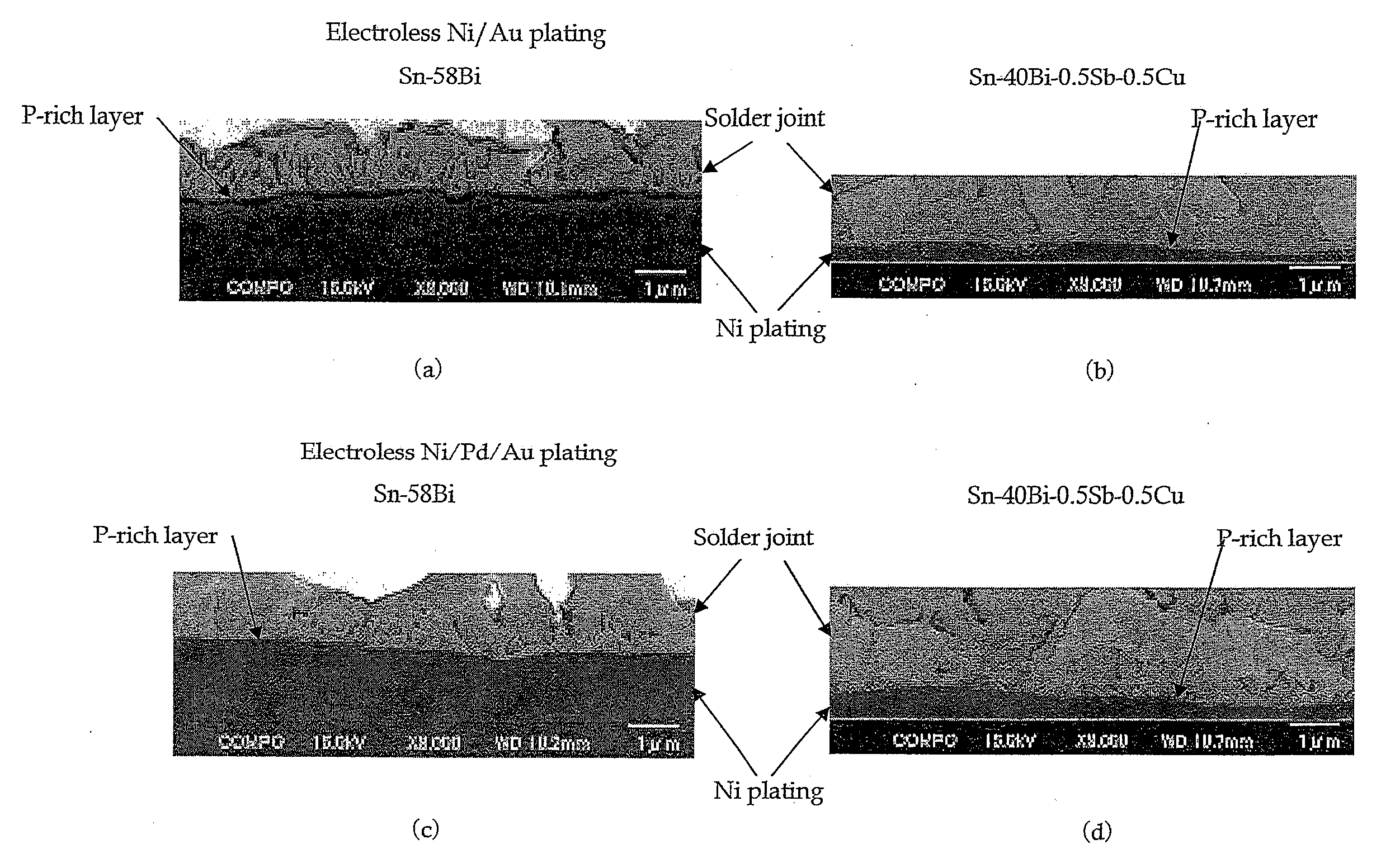
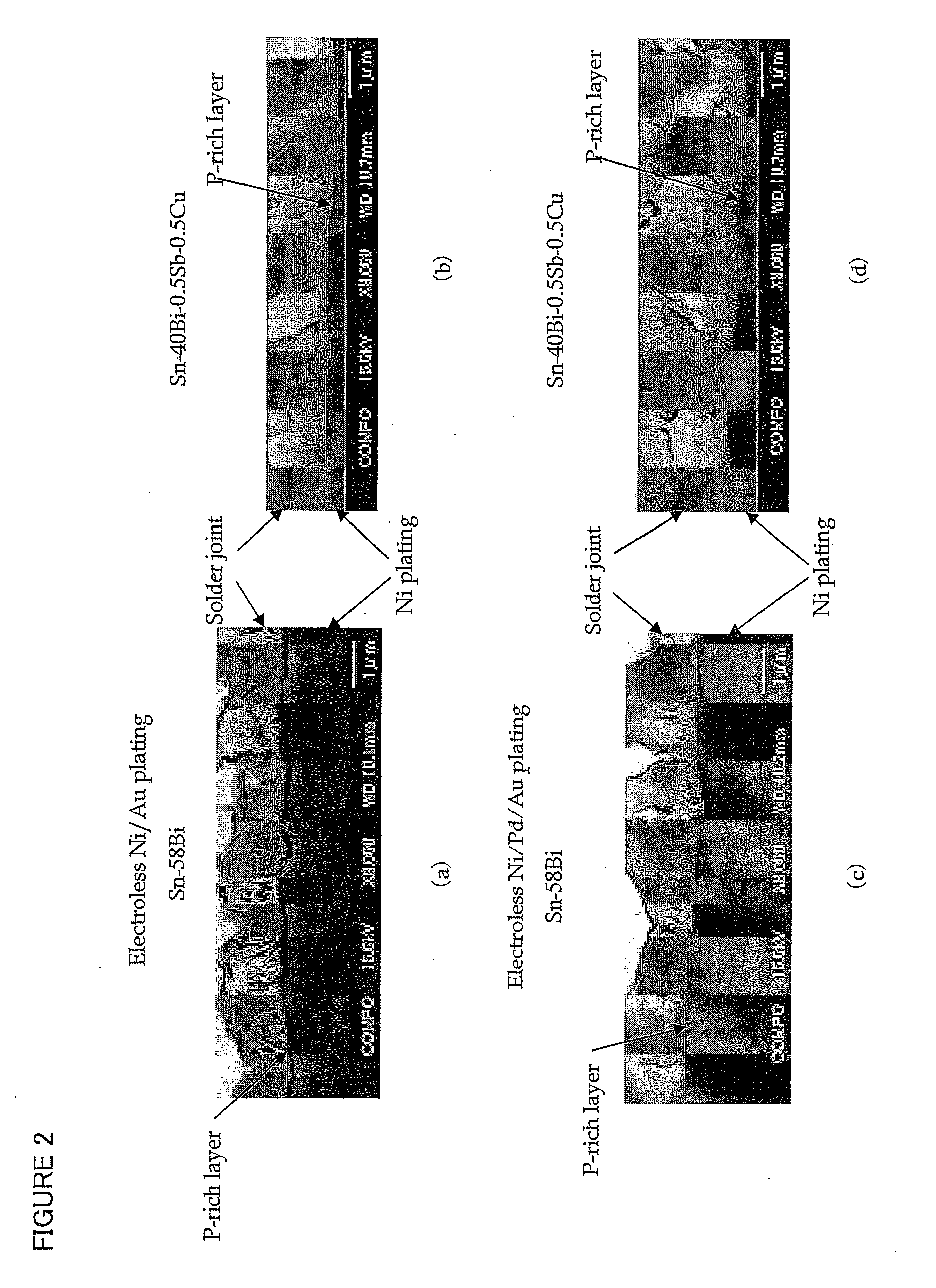
The P-rich layer is hard and brittle, and it deteriorates the shear strength of a solder joint.
Therefore, the formation of a P-rich layer adversely affects the bonding reliability of a solder joint.

Method used


Image

  • Lead-Free Solder Alloy
  • Lead-Free Solder Alloy
  • Lead-Free Solder Alloy

Examples


examples

[0044]The solder alloys having compositions shown in Table 1 were prepared. The melting point, the tensile strength, the elongation (ductility), the thickness of a P-rich layer, the shear strength, and the percent exposure of plating were determined for these solder alloys as described below. The results are also shown in Table 1.

Melting Point of the Solder Alloy

[0045]The melting point (° C.) of each solder alloy was measured using a differential scanning calorimeter (DSC) (Model DSC 6200 of Seiko Instruments, Inc.) at a rate of temperature increase of 5° C. per minute.

Tensile Strength and Elongation (Ductility)

[0046]The solder alloys having compositions shown in Table 1 were formed into test specimens for a tensile test, and the tensile strength (MPa) and the elongation (%) of the specimens were measured using a tensile strength tester (Auto Graph AG-201kN manufactured by Shimadzu Corporation) at a stroke speed of 6.0 mm per minute and a strain rate of 0.33% per second. A solder al...


PUM

PropertyMeasurementUnit
Fractionaaaaaaaaaa
Fractionaaaaaaaaaa
Fractionaaaaaaaaaa

Abstract

A lead-free solder alloy consisting essentially of, in mass percent, Bi: 31-59%, Sb: 0.15-0.75%, at least one element selected from Cu: 0.3-1.0% and P: 0.002-0.055%, and a balance of Sn has a low melting point for suppressing warping of a thin substrate during soldering. It can form solder joints with high reliability even when used for soldering to electrodes having a Ni coating which contains P, since the growth of a P-rich layer is suppressed so that the shear strength of the joints is improved and the alloy has a high ductility and a high tensile strength.

Description

TECHNICAL FIELD[0001]This invention relates to a Sn—Bi—Sb based lead-free solder alloy and particularly a Sn—Bi—Sb based lead-free solder alloy having excellent bonding reliability.BACKGROUND ART[0002]In recent years, electronic equipment such as cellular phones is becoming smaller and thinner. In electronic parts such as semiconductor devices used in such electronic equipment, thin substrates having a thickness from around several millimeters to 1 mm or less are now being used.[0003]Sn—Ag—Cu solder alloys have been widely used as lead-free solders. Sn—Ag—Cu solder alloys have a relatively high melting point, which is around 220° C. even for a eutectic Sn-3Ag-0.5Cu solder alloy. Therefore, when soldering of electrodes to thin substrates like those described above is carried out using a Sn—Ag—Cu solder alloy, the substrates sometimes warp due to the heat at the time of soldering, leading to the occurrence of bonding defects.[0004]As a countermeasure against such bonding defects, warp...

Claims


Application Information

Patent Timeline
IPC IPC(8): B23K35/26
CPCB23K35/262B23K2201/38B23K35/264B32B15/01B32B15/018C22C12/00C22C13/02B23K2101/38
Inventor TACHIBANA, KENNOMURA, HIKARULEE, KYU-OH
Owner SENJU METAL IND CO LTD
Learn More