

Image sensor and electronic device including the same
a technology of image sensor and electronic device, which is applied in the direction of radio frequency controlled devices, instruments, semiconductor devices, etc., can solve the problems of reducing the area absorbing light in each pixel to about 13, deteriorating sensitivity, and substantial light loss, so as to improve the sensitivity and optical efficiency, enhance the wavelength selectivity of each pixel, and increase the area absorbing light
Active Publication Date: 2015-02-12
SAMSUNG ELECTRONICS CO LTD
View PDF3 Cites 5 Cited by
- Summary
- Abstract
- Description
- Claims
- Application Information
AI Technical Summary
Benefits of technology
The patent describes an improved image sensor that can capture more light and select specific colors for each pixel. This results in better sensitivity and more efficient optics.
Problems solved by technology
At present, a silicon photodiode is widely used, but it may have a deteriorated sensitivity because it has a small absorption area due to small pixels.
However, because the color filter absorbs light by itself, a substantial amount of light is lost while being transferred to the photodiode, and the area absorbing light in each pixel is decreased to about ⅓ when including, for example, a red pixel, a blue pixel, and a green pixel, so that each pixel uses only about ⅓ of available light.
Method used
View moreImage
Smart ImageViewing Examples

Examples
example 1
[0081]An image sensor is supposed under the following simulation conditions, and light transmittance and wavelength selectivity are anticipated.
[0082]Simulation Conditions[0083]Nanostructural body: stepped nanostructural body having a first width (long width) of 0.32 μm, a second width (short width) of 0.16 μm, a first length (long length) of 1.2 μm, a second length (short length) of 0.6 μm, a thickness of 2 μm, and a distance (H) from an upper end of the nanostructural body to the light detector of 2.6 μm,[0084]Focusing lens: Gaussian shape[0085]Photoelectric device: ITO 100 nm / N,N-dimethylquinacridone (Chemical Formula 1a)+dicyanovinyl-terthiophene (Chemical Formula 2a) (1:1 wt / wt, 70 nm) / aluminum 80 nm
Login to View More PUM
 Abstract
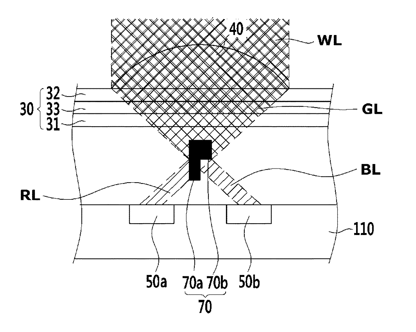
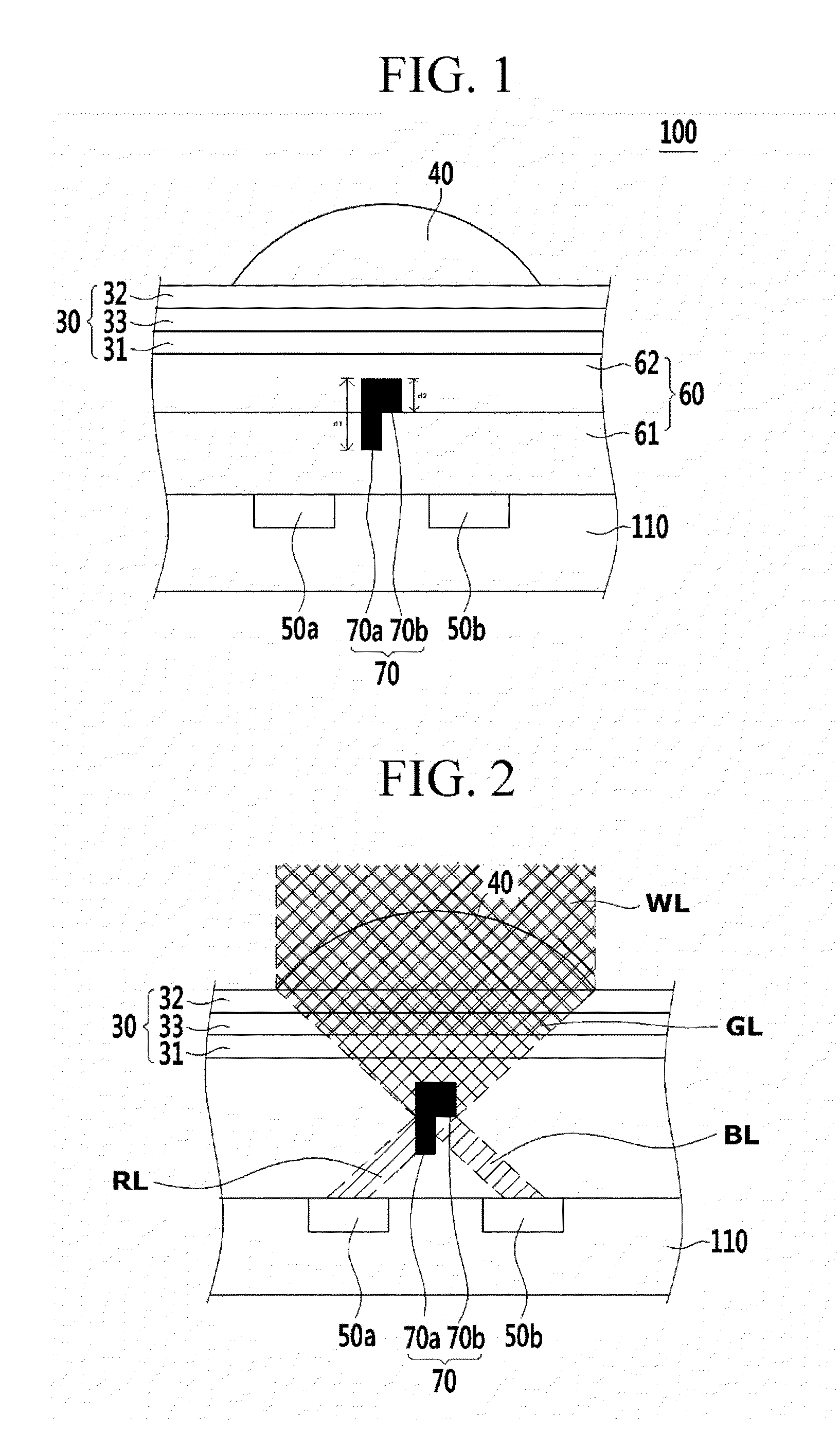
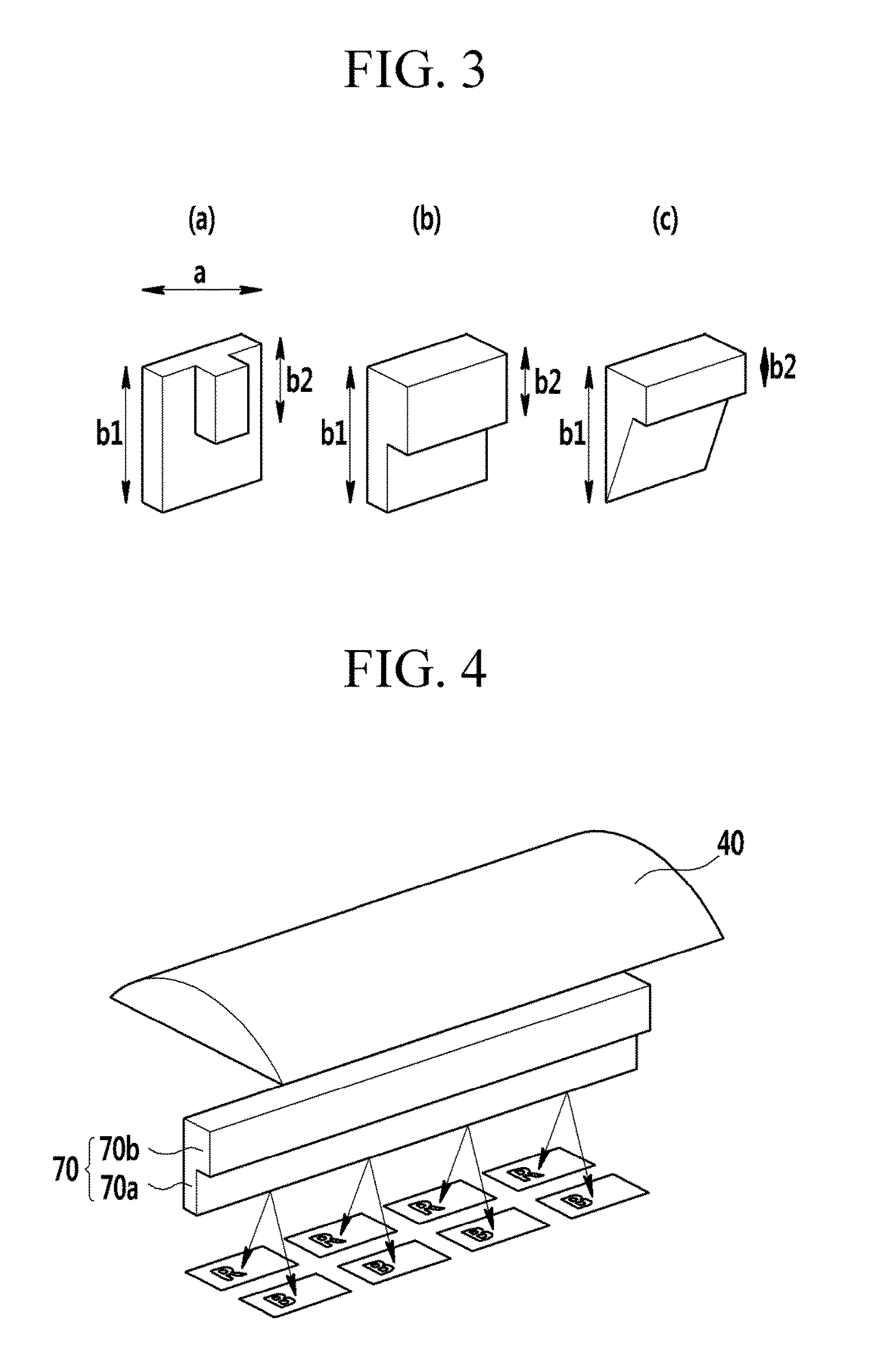
An image sensor includes a semiconductor substrate integrated with at least one first photo-sensing device sensing light in a first wavelength region and at least one second photo-sensing device sensing light in a second wavelength region shorter than the first wavelength region, a photoelectric device including a pair of electrodes facing each other and a light absorption layer between the electrodes, the photoelectric device selectively absorbing light in a third wavelength region between the first wavelength region and the second wavelength region, and a nanostructural body between the semiconductor substrate and the photoelectric device, the nanostructural body including at least two parts having different optical paths.
Description
CROSS REFERENCE TO RELATED APPLICATION[0001]This application claims priority to and the benefit of Korean Patent Application No. 10-2013-0093281 filed in the Korean Intellectual Property Office on Aug. 6, 2013, the entire contents of which are incorporated herein by reference.BACKGROUND[0002]1. Field[0003]Example embodiments are related to an image sensor and an electronic device including the same.[0004]2. Description of the Related Art[0005]A photoelectric device converts light into an electrical signal using photoelectric effects, and may include a photodiode and / or a phototransistor, and may be applied to an image sensor and / or a solar cell.[0006]An image sensor including a photodiode requires high resolution and thus a small pixel. At present, a silicon photodiode is widely used, but it may have a deteriorated sensitivity because it has a small absorption area due to small pixels.[0007]On the other hand, a color filter may be used for selectively absorbing light in a predetermi...
Claims
Login to View More Application Information
Patent Timeline
 Patent Type & AuthorityApplications(United States)
IPC IPC(8): H01L31/0232
CPCH01L31/0232H01L27/14629H01L27/14645H01L27/14621H01L31/02327H01L27/14625H01L27/14627H01L27/146H01L31/02H10K39/32G02B27/1013
InventorLEE, GAE HWANGKIM, KYU SIKJIN, YONG WAN
OwnerSAMSUNG ELECTRONICS CO LTD