
Polyurethane polishing pad

a technology of polyurethane and polishing pads, which is applied in the field of polishing pads, can solve the problems of lack of planarization and copper dishing properties of the polishing pads produced from these formulations

Inactive Publication Date: 2015-03-05
DOW GLOBAL TECH LLC +1
View PDF1 Cites 9 Cited by
  • Summary
  • Abstract
  • Description
  • Claims
  • Application Information

AI Technical Summary

Benefits of technology

The invention provides a polishing pad suitable for planarizing semiconductor, optical, and magnetic substrates. The pad is made from a specific type of polyurethane material that has been formed and cured using a curative agent. The result is a non-porous pad with specific properties that make it effective for polishing different materials. The technical effect of the invention is to provide a consistent and high-quality polishing pad that can be used for a variety of substrates, increasing the efficiency and effectiveness of the polishing process.

Problems solved by technology

Unfortunately, polyurethane pads produced from these formulations lack the planarization and copper dishing properties necessary for the most demanding low defect polishing applications.

Method used


Image

  • Polyurethane polishing pad

Examples


example 1

[0023]Table 1 includes the formulations for a series of pads manufactured to the above method with various prepolymers, isocyanate amounts and curatives.

TABLE 1Adiprene ® and Vibrathane ® are urethane prepolymer products of Chemtura Corporation all NCO values represent nominal amounts.UnreactedIsocyanateNCOStoichiometryFormulationPolyol BackbonePrepolymerWt. %Curative(%)A-1PTMEGAdiprene LF750D8.9MOCA85B-1PTMEGAdiprene LF750D8.9MOCA105C-1PTMEGAdiprene LF750D8.9MOCA115D-1PTMEG / PPGAdiprene LF750D / 8.8MOCA95LFG740DE-1PTMEG / PPGAdiprene LF750D / 7.3MOCA97LFG963AF-1PPGVibrathane B6284.2MOCA95F-2PPGVibrathane B6284.2MOCA105G-1PTMEGAdiprene LF900A3.8MOCA95G-2PTMEGAdiprene LF900A3.8MOCA105H-1PTMEGAdiprene LF800A2.9MOCA95H-2PTMEGAdiprene LF800A2.9MOCA105I-1PPGAdiprene LFG963A5.75MOCA90I-2PPGAdiprene LFG963A5.75MOCA102.51PPGAdiprene LFG963A5.75MCDEA102.52PPGAdiprene LFG963A5.75MCDEA110E-2PTMEG / PPGAdiprene LF750D / 7.3MCDEA110LFG963AE-3PTMEG / PPGAdiprene LF750D / 7.3MCDEA110LFG963AJ-1PPGAdiprene LFG963A...

example 2

[0027]Porous formulations of pad samples used in bulk copper polishing tests were modified as illustrated in Table 3.

TABLE 3EXPANCELEstimatedUnreactedPolymerMicrosphereNCOMicrospheresMicrosphereDensityFormulationWt. %CurativeStoichiometry %(Diameter)Wt. %(g / cc)1-A5.75MCDEA102.5461DE20d701.920.070(20 μm)I-15.75MOCA90551DE40d421.120.042(40 μm)E-47.3MOCA97551DE20d602.060.060(20 μm)L-18.8MOCA95551DE20d601.350.060(20 μm)

[0028]A polishing defect comparison was then completed between formulation 1A and comparative formulation E-4. The pads Polishing conditions were with grooves having a depth of 30 mils (0.760 mm), width of 18 mils (0.457 mm) and a pitch of 70 mils (1.778 mm) on an Applied Materials Reflection LK tool, with a wafer velocity of 87 rpm and a platen velocity of 93 rpm using in-situ conditioning with a Kinik AD3BG-150855 diamond conditioner using Planar Solution CSL9044C slurry. Copper blanket wafers were inspected using KLA-Tencor Surfscan SPITBI with a threshold at 0.07 micr...

example 3

[0030]The pads of Table 3 were then tested for dishing on an Applied Material Reflexion LK tool. Tables 5 and 6 below provides dishing at various densities after 60 seconds over polishing.

TABLE 5StoicPorosity10 × 10 μm50 × 50 μm100 × 100 μmFormulationPrepolyrnerCurative(%)(vol. %)(No.)(No.)(No.)E-4LF750D / LFG963AMOCA97325347568501-ALFG963AMCDEA102.524447484538L-1LFG740DMOCA95325859051050

TABLE 6StoicPorosity7 × 3 μm9 × 1 μm100 × 1 μmFormulationPrepolymerCurative(%)(vol. %)(No.)(No.)(No.)E-4LF750D / LFG963AMOCA973254778014061-ALFG963AMCDEA102.524481605676L-1LFG740DMOCA95325408301650

[0031]Tables 5 and 6 show the MCDEA pad of the invention having the best dishing performance at the densities tested. Since pads with low defects often have higher dishing, this represents an unexpected feature of the invention. Additional tests have shown that a stoichiometry of 100 to 112 percent provides the best dishing performance and exhibits the best topography performance.


PUM

PropertyMeasurementUnit
Temperatureaaaaaaaaaa
Percent by massaaaaaaaaaa

Abstract

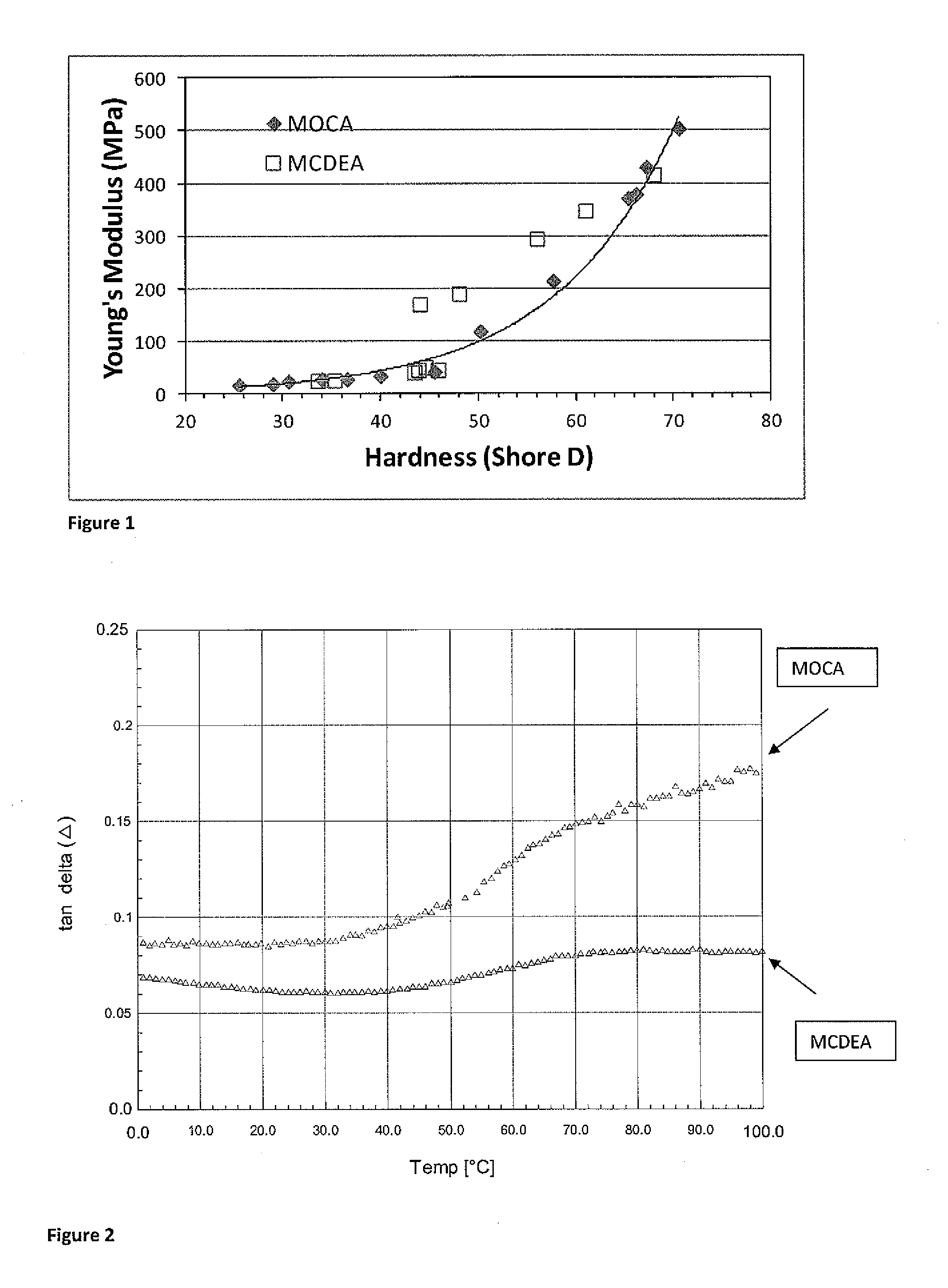
The invention provides a polishing pad suitable for planarizing semiconductor, optical and magnetic substrates. The polishing pad includes a cast polyurethane polymeric material formed from a prepolymer reaction of a polypropylene glycol and a toluene diisocyanate to form an isocyanate-terminated reaction product. The toluene diisocyanate has less than 5 weight percent aliphatic isocyanate; and the isocyanate-terminated reaction product having 5.55 to 5.85 weight percent unreacted NCO. The isocyanate-terminated reaction product being cured with a 4,4′-methylene-bis(3-chloro-2,6-diethylaniline) curative agent. The non-porous cured product having a tan delta of 0.04 to 0.10, a Young's modulus of 140 to 240 MPa and a Shore D hardness of 44 to 56.

Description

BACKGROUND[0001]This specification relates to polishing pads useful for polishing and planarizing substrates and particularly to planarizing polishing pads producing low defect levels.[0002]Polyurethane polishing pads are the primary pad-type for a variety of demanding precision polishing applications. These polyurethane polishing pads are effective for polishing silicon wafers, patterned wafers, flat panel displays and magnetic storage disks. In particular, polyurethane polishing pads provide the mechanical integrity and chemical resistance for most polishing operations used to fabricate integrated circuits. For example, polyurethane polishing pads have high strength for resisting tearing; abrasion resistance for avoiding wear problems during polishing; and stability for resisting attack by strong acidic and strong caustic polishing solutions.[0003]The production of semiconductors typically involves several chemical mechanical planarization (CMP) processes. In each CMP process, a p...

Claims


Application Information

Patent Timeline
IPC IPC(8): B24B37/24
CPCB24B37/24B24B37/245C08G18/10C08G18/12C08G18/40C08G18/48C08G18/66C08G18/76
Inventor YEH, FENGJIDEGROOT, MARTY W.MURNANE, JAMESJAMES, DAVID B.KULP, MARY JO
Owner DOW GLOBAL TECH LLC
Learn More