Controlled impedance PCB encapsulation

Inactive Publication Date: 2015-03-19
BT ENG
View PDF8 Cites 5 Cited by
  • Summary
  • Abstract
  • Description
  • Claims
  • Application Information

AI Technical Summary

Benefits of technology

The invention provides a method for creating coatings that offer complete EMI shielding, are cost-effective to produce, are lighter than other coatings, have lower manufacturing complexity, and enable higher electrical circuit densities while also improving isolation and noise suppression.

Problems solved by technology

None of the previous teachings describe deposition methods that can produce controlled impedance conformal coatings.
The previous teachings and prior art provide for conformal conducting layer layers of insufficient quality so that complete EMI shielding is impractical.
While the use of loaded or intrinsically conducting polymers produce coatings which must either be impractically thick to stop EMI due to excessive skin depths.
A significant deficiency of prior teaching which do not indicate gas-phase conformal encapsulation, but rather coating techniques from liquid phase is the fact that such deposition techniques often leave behind large occlusions in the surface.
For a 2 GHz impinging frequency, the gap size is impractically small if vapor phase deposition techniques are not used.
Another deficiency of previous teachings is also due to lack of conformality of the coating techniques disclosed as means to produce EMI shields.
In techniques involving dipping, painting, or spraying small pockets are formed that leave high stress points that cause failures when the coated samples are heated and cooled due to typical use condition.
Sputtering or other means of physical vapor deposition impose difficult to control stresses as the coating layer grows.
These stresses and non-uniformities due to shadowing of the surface by three dimensional parts also cause delamination failures when coated samples undergo heating and cooling.

Method used


Image

  • Controlled impedance PCB encapsulation
  • Controlled impedance PCB encapsulation
  • Controlled impedance PCB encapsulation

Examples


Embodiment Construction

[0021]The invention is described here in terms of preferred embodiments, structures, and method steps, however, it will be understood that substitutions and equivalents as will be apparent to those of ordinary skill in the art may be used without departing from the scope of the invention as defined by the appended claims.

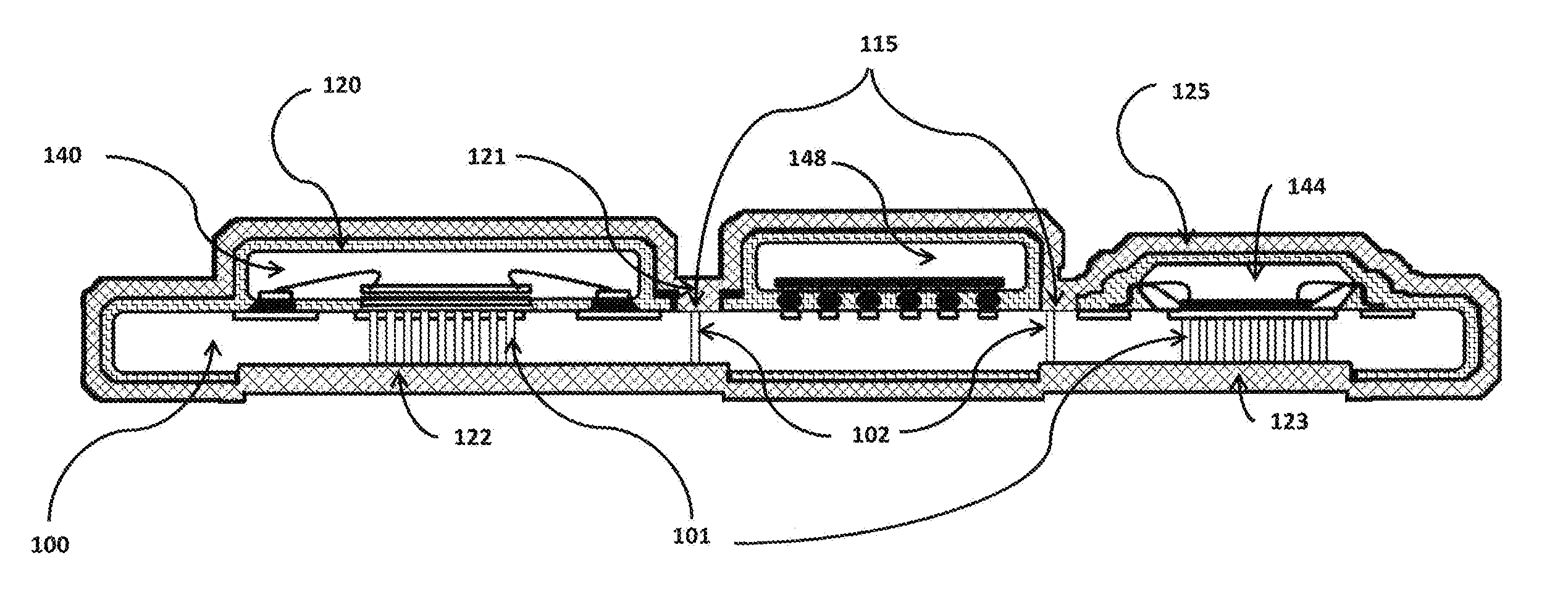
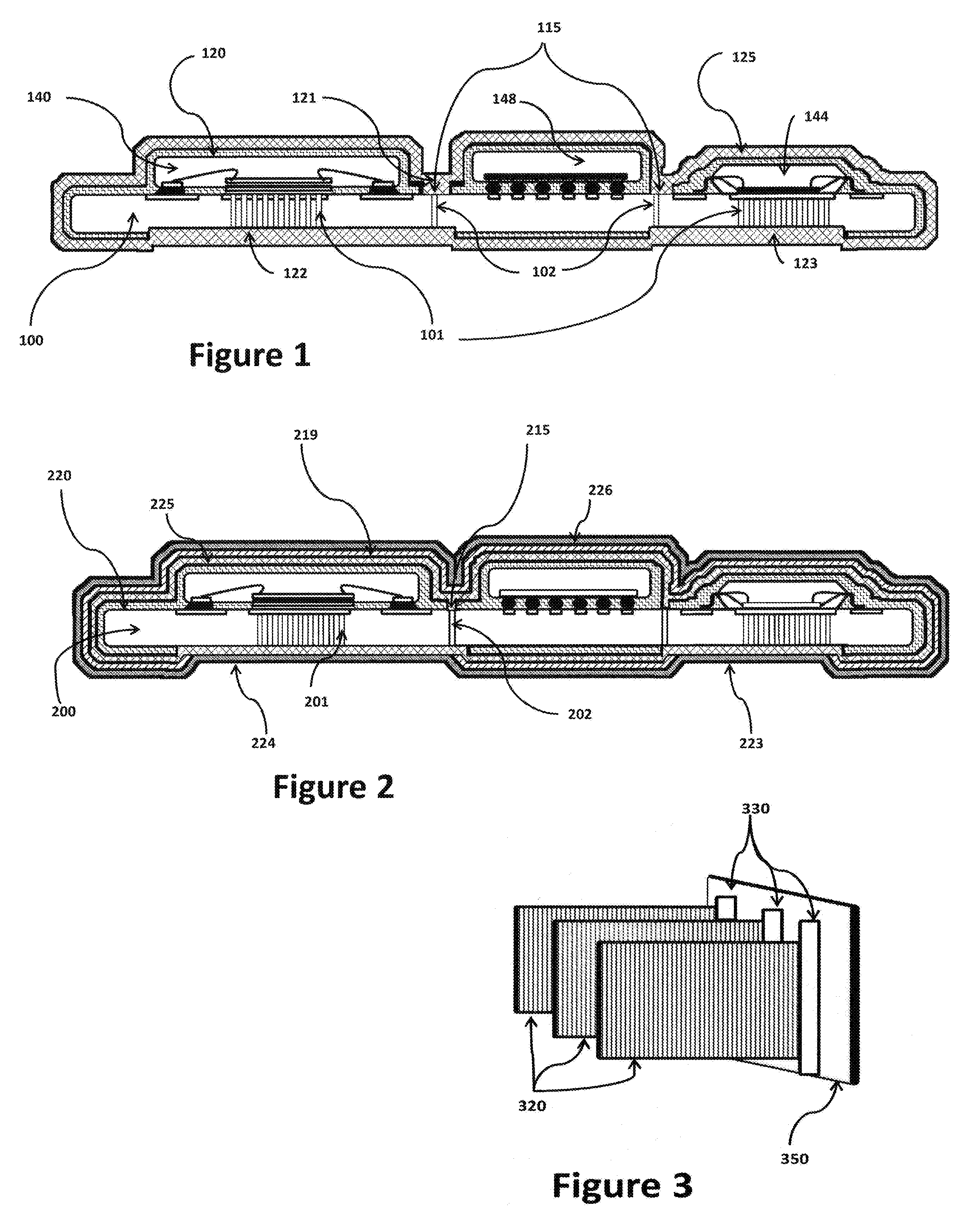
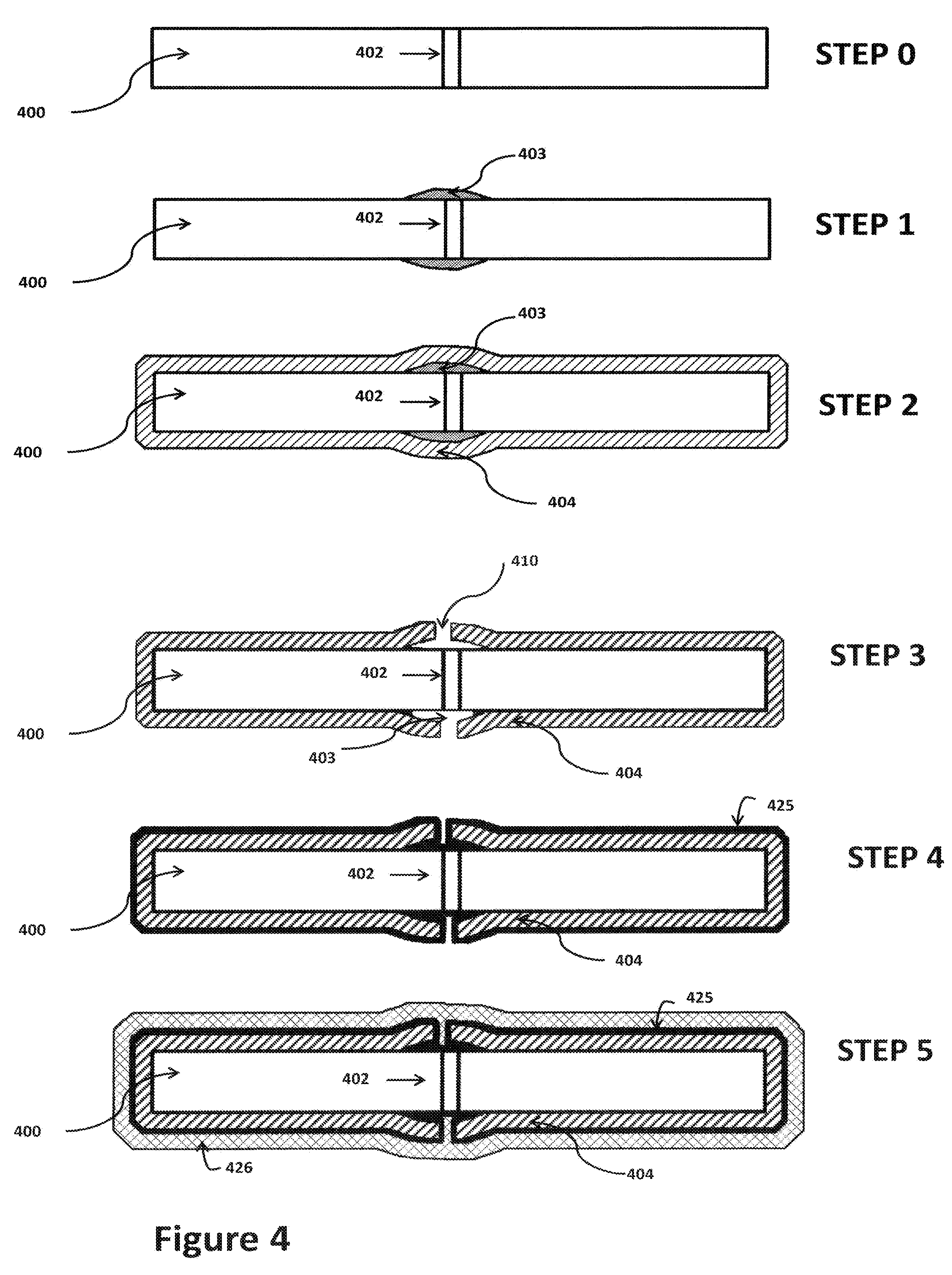
[0022]According to the invention, a device comprised of a printed circuit board (100 in FIG. 1) populated with integrated circuits, has a non-conductive coating layer, 120, formed from a gas-phase deposition process which conformally encapsulates printed circuit board, 100, and all of the integrated circuits in their entirety. To be a gas-phase derived product, the coating process must occur under reduced pressure so that the molecules forming the coating have sufficient diffusion lengths so as to coat beneath surfaces.

[0023]This is typically accomplished using a vacuum. Subsequently, a gas-phase phase derived conductive coating, 125, encapsulates the entirety of th...


PUM


Abstract

The present invention discloses methods and devices for encapsulating PCBs, assemblies of PCBs, and their electronic components. The encapsulation methods disclosed can be used to produce electromagnetic shields whose impedance is controlled.

Description

[0001]This application claims the benefit of U.S. Provisional Patent Application No. 61 / 591,942, filed Jan. 29, 2012.BACKGROUND OF THE INVENTION[0002]The present invention relates to methods for encapsulating electronic assemblies. As an example, the invention teaches methods for completely encapsulating a printed circuit board and all of its components within a nonconductive coating whose layer thickness is precisely controlled and subsequently encapsulating the previously encapsulated assembly within a conformal conductive coating.[0003]Coating and shielding electronic components and assemblies serve many purposes. One is to reduce the effects of water and corrosive agents on the electronic components. Another is to provide electromagnetic interference shielding, known as EMI shielding, from external electromagnetic radiation sources. Yet another is to eliminate noise between components. Various patents teach methods to shield circuit boards U.S. Pat. No. 5,696,196 teaches of an a...

Claims


Application Information

Patent Timeline
IPC IPC(8): H05K9/00H05K1/18
CPCH05K1/181H05K9/00H05K1/0206H05K1/0218H05K1/0243H05K3/14H05K3/284H05K2201/0715
Inventor THIESEN, JACKBRAKORA, KARL
Owner BT ENG
Why Eureka
Try Eureka