NAND array hiarchical bl structures for multiple-wl and all-bl simultaneous erase, erase-verify, program, program-verify, and read operations

a nand array and bl structure technology, applied in static storage, digital storage, instruments, etc., can solve the problems of short data retention life cycle, low program, erase and read cycle, high power consumption, etc., and achieve the highest read speed, fast read speed, and large channel width

Active Publication Date: 2015-03-19
APLUS FLASH TECH
View PDF5 Cites 25 Cited by
  • Summary
  • Abstract
  • Description
  • Claims
  • Application Information

AI Technical Summary

Benefits of technology

[0063]The 35th objective of the present invention is to disclose all above proposed 2-level broken BL HiNAND2 array can be reduced to 1-level broken BL HiNAND1 array only with metal1 broken GBL lines for different and high-density memories such as NOR array, SARAM array, DRAM array, PLD array, CAM array, and ROM array. This 1-level divided GBL architecture with segmented DGBL capacitance would result in faster read speed....

Problems solved by technology

The reliability issues include short data retention life cycle, high power-consumption and low Program, Erase and Read cycles.
Although a 3D NAND flash memory has many advantages to use the less advanced technology nodes to increase NAND density over 1 Tb with a smaller silicon area than 2D NAND, it encounters new process disadvantages such as high aspect ratio, stair-case etching etc, more WL disturbance and new challenges to use the new scheme of gate-induced-d...

Method used


Image

  • NAND array hiarchical bl structures for multiple-wl  and all-bl simultaneous erase, erase-verify, program, program-verify, and read operations
  • NAND array hiarchical bl structures for multiple-wl  and all-bl simultaneous erase, erase-verify, program, program-verify, and read operations
  • NAND array hiarchical bl structures for multiple-wl  and all-bl simultaneous erase, erase-verify, program, program-verify, and read operations

Examples


case1

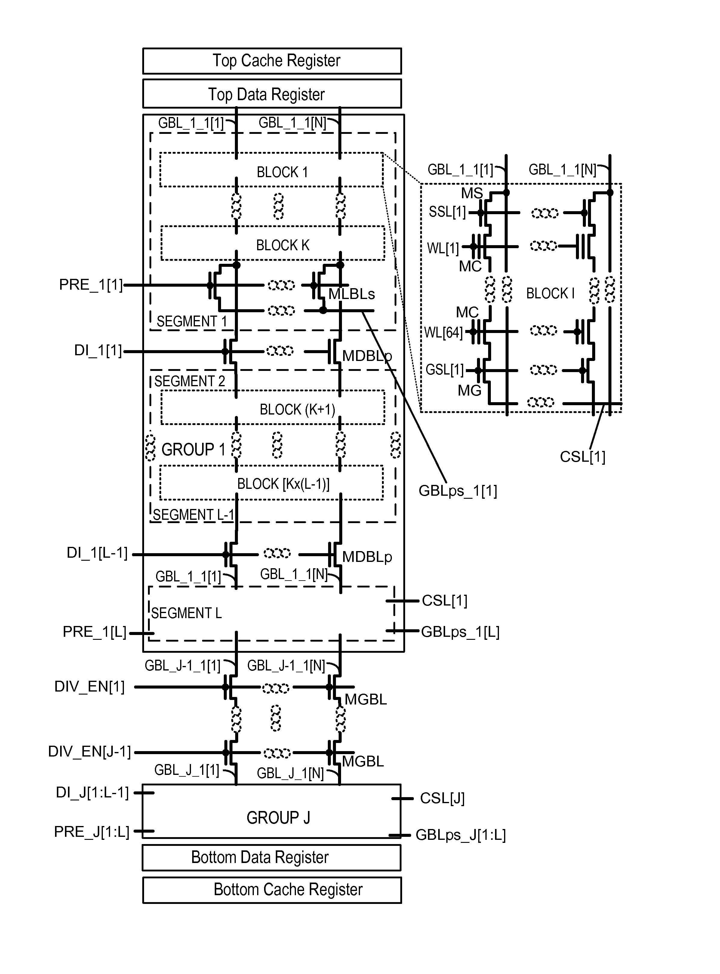
[0305] Each WL data of Vss-program and Vdd-inhibit voltages are coupled directly from a N-bit PB to one selected N-bit Block at a time. These Vss and Vdd voltages are passed to the selected channels through N selected broken GBLs, through N selected MLBLp transistors in on-state to N broken LBL lines and then to N Selected NAND Strings through N first String-select transistors MS in on-state and N second String-select transistor MG in off-state to prevent the String leakage. All this Vdd-inhibit and Vss programmed voltages are then latched or trapped in the selected N CSEG capacitors in the selected Segment and Group in accordance with the WL data stored in the N-bit PB. After this medium CSEG capacitors are precharged with one-shot of Vdd-inhibit and Vss, the N gates of LBL-select transistors MLBLp are then being shut off by setting SEG signal to Vss to trap Vdd-inhibit and Vss. This precharged process takes time less than 200 ns to 3 μs, depending on the Block location or distance...

case2

[0307] In this case, all selected CSEG capacitors are precharged with 7V-inhibit voltage initially by coupling the selected 64 LBLps lines (respectively associated with 64 Segments in dispersed Groups) to 7V with PRE being set to 7V+Vt+Vmargin, where Vmargin˜0.5V. For this case, PRE signal is at Vpass˜10V.

[0308]The precharge cycle is similar for charging N broken CGBL capacitors with Vdd-inhibit and Vss voltages as in Case1 which are coupled from a N-bit PB in accordance with the stored WL-data pattern. Then SEG signal is switched from Vss to Vdd to turn on MLBLp transistors to connect each broken CGBL capacitor to each corresponding CSEG capacitor that is filled with the precharged 7V-inhibit initially. As a result, the voltages of LBL capacitors will be selectively discharged to either Vss or retained to 7V-inhibit voltage according to VGBL=Vss and VGBL=Vdd from the PB respectively through transistors MLBLp set to On-state.

[0309]In other words, both Case1 and Case2 need the Vdd-in...

second embodiment

[0392]FIG. 17 is a simplified circuit diagram showing a 3D HiNAND2 array with 3-transistor divided-GBL / LBL device and U-shaped vertical String according to another embodiment of the present invention. It is 3D HiNAND2 circuit with divided GBL devices for the broken GBLs and broken LBLs. The divided GBL devices include one paired NMOS transistors of MGBLp with a common gate connected to DIV_EN and one Back-gate NMOS transistor of MC with its gate tied to BG. Similarly, the divided LBL devices are comprised of one paired transistors of MLBLp with a common gate tied to DI—1 and one back-gate NMOS transistor, MC, with gate tied to BG—[1].

[0393]Besides the one divided device is added in between two adjacent broken GBL capacitors and two adjacent broken LBL capacitors, there are additional devices are added at one end of each LBL and each GBL. These devices are like the above said devices for the Divided or broken LBL and GBL.

[0394]For example, these devices include one-paired MLBLps with...


PUM


Abstract

Several 2D and 3D HiNAND flash memory arrays with 1-level or 2-level broken BL-hierarchical structures are provided for Multiple Whole-WL and All-BL simultaneous operations in Dispersed Blocks. The global bit line (GBL) is divided to multiple 1(top)-level broken metal2 GBLs plus optional lower-level broken metal1 local bit lines (LBLs). A preferred Vinhibit supply higher than Vdd can be selectively supplied via horizontal metal0 power line LBLps to charge selected broken GBLs/LBLs which can also be selectively discharged via a String source line. Charge-sharing technique for precharging and discharging of broken GBL/LBL capacitors for NAND cell data sensing is used in Read and Verify operations with reduced power consumption and latency. Recall technique to restore the desired Program Data stored in the broken GBL/LBL capacitors is used for Multiple-WL and All-BL Program and Program-Verify operation with reduced program current for highest program yield superior P/E cycles.

Description

1. CROSS-REFERENCES TO RELATED APPLICATIONS[0001]This application claims priority to U.S. Provisional Application No. 61 / 858,611, filed Jul. 25, 2013, commonly assigned and incorporated by reference herein for all purposes.[0002]Additionally, this application is related to U.S. patent application Ser. No. 14 / 316,936, filed Jun. 27, 2014, and U.S. patent application Ser. No. 14 / 283,209, filed May 20, 2014, commonly assigned and incorporated by references herein for all purposes.[0003]This application is also related to U.S. Patent Application No. 2012 / 0051137 A1, U.S. Pat. No. 8,189,391, U.S. Pat. No. 8,169,826, U.S. Pat. No. 8,194,453, U.S. Pat. No. 8,203,882, U.S. Pat. No. 8,334,551, U.S. Pat. No. 8,148,763, U.S. Pat. No. 8,335,111, U.S. Pat. No. 8,437,192, and U.S. Pat. No. 8,461,000, and U.S. Pat. No. 8,488,382 on 3D NAND array architecture and operation.2. BACKGROUND OF THE INVENTION[0004]The present invention generally relates to advanced NAND memory technology. More specifical...

Claims


Application Information

Patent Timeline
IPC IPC(8): G11C11/56G11C16/34G11C16/26G11C16/10G11C16/16
CPCG11C11/5635G11C11/5642G11C16/3459G11C16/16G11C16/26G11C16/10G11C11/5628G11C16/0483G11C16/06G11C16/3418G11C2211/5641G11C11/56G11C11/5671G11C16/14G11C16/24
Inventor LEE, PETER WUNG
Owner APLUS FLASH TECH
Why Eureka
Try Eureka