Molecular Organometallic Resists for EUV

a technology of organometallic resists and euv, which is applied in the field of thin films, can solve the problems of poor manufacturing through-put, higher manufacturing cost, and general unsuitability of phenolic materials commonly used for photolithography using light wavelength 248 nm wavelength

Active Publication Date: 2015-03-19
THE RES FOUND OF STATE UNIV OF NEW YORK
View PDF10 Cites 41 Cited by
  • Summary
  • Abstract
  • Description
  • Claims
  • Application Information

AI Technical Summary

Problems solved by technology

For example, phenolic materials which are commonly used for photolithography using light of wavelength 248 nm wavelength are generally not suitable for use as photoresists for light of 193 nm, since these phenolic materials tend to absorb too much 193 nm light.
Conversely, if too little light is absorbed, then the exposure times will need to be long, resulting in poor manufacturing through-put, and higher manufacturing costs.
In order to do so, the photoresists have to become thinner and thinner, but as they become thinner, it becomes harder to stop photons.

Method used


Image

  • Molecular Organometallic Resists for EUV
  • Molecular Organometallic Resists for EUV
  • Molecular Organometallic Resists for EUV

Examples


Embodiment Construction

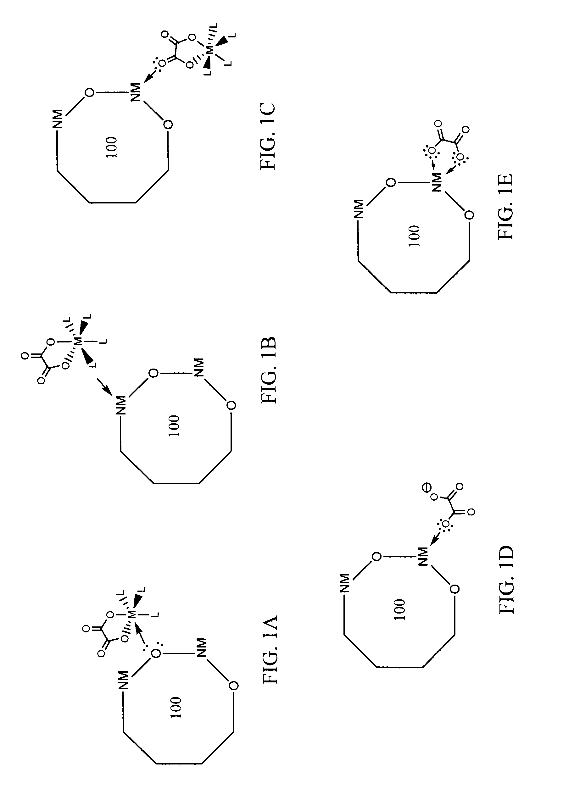
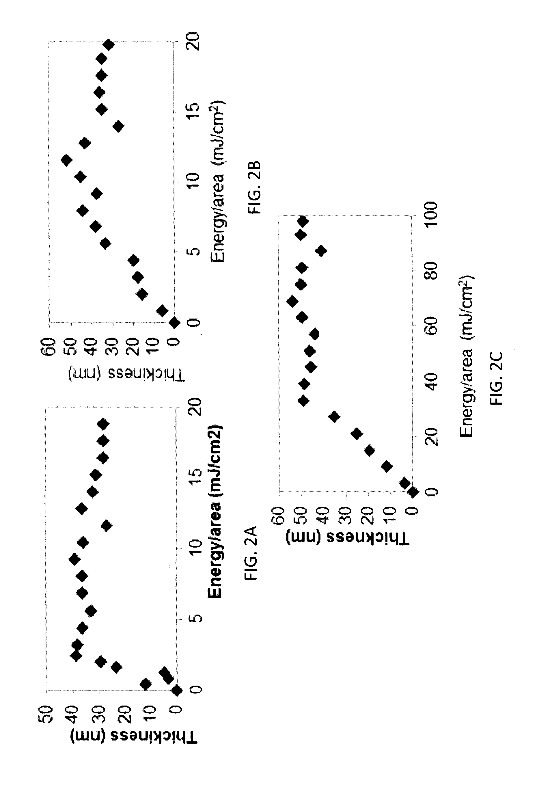
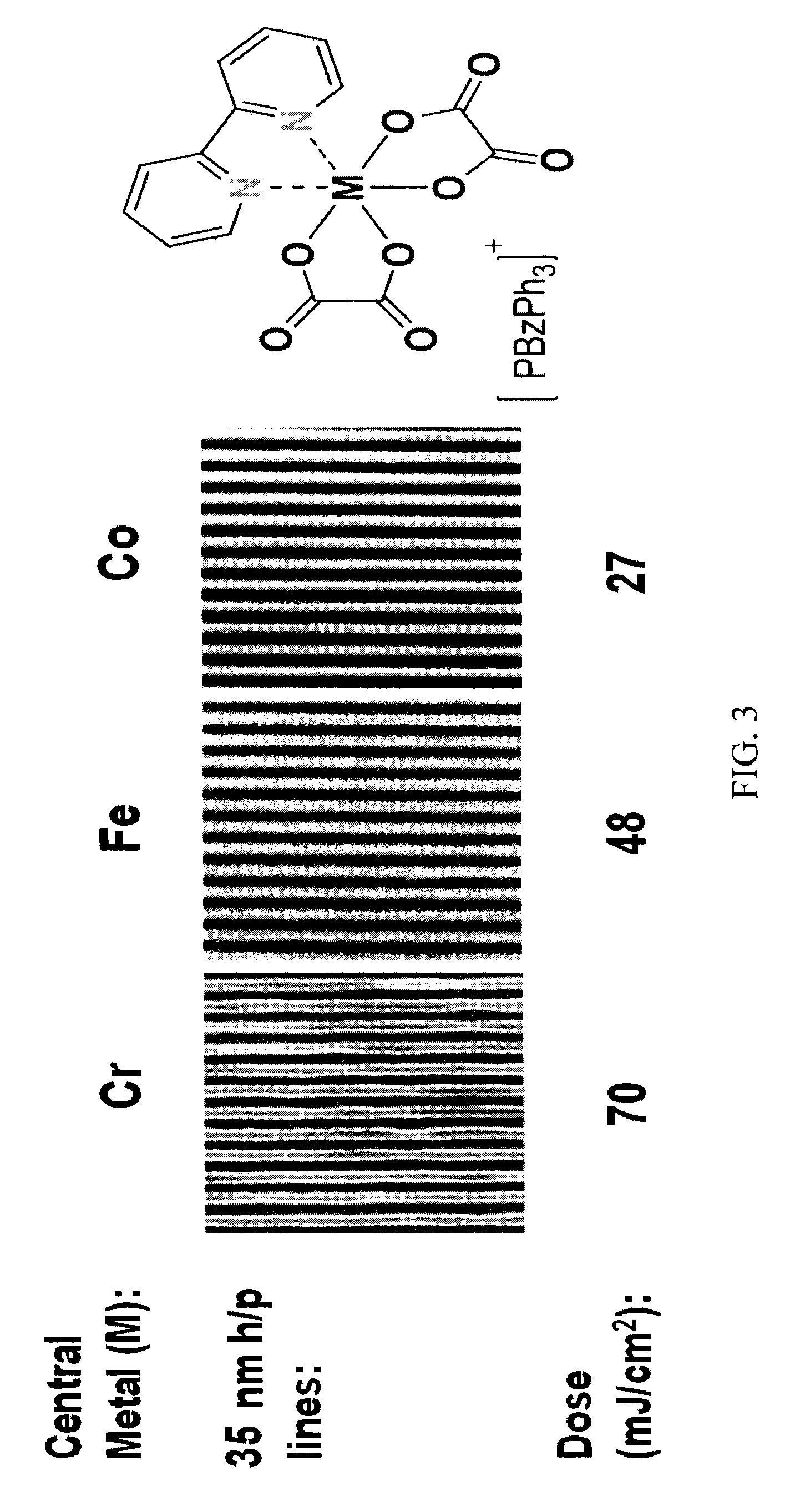
[0016]This disclosure relates to a platform of photoresists that includes high optical density organometallic complexes. These materials possess the capability of stopping EUV photons in 20-nm films (high EUV OD) and converting the photons into secondary electrons with short diffusion lengths, causing a photochemical change that will result in negative- or positive-tone imaging.

[0017]The potential benefits of these resists are many. Organometallic films with high extreme ultraviolet optical density are able to stop more photons, thus, by utilizing these materials, thin film resists can be made without loss to sensitivity or line edge roughness. Line edge roughness increases as acid diffuses into the unexposed region, leading to a loss of resolution; however, since metals have a large range of redox potentials, the chemistry of these resists can be engineered for high sensitivity without acid catalysis, limiting potential acid diffusion problems. These materials also possess a high m...


PUM

PropertyMeasurementUnit
diameteraaaaaaaaaa
diameteraaaaaaaaaa
wavelength 248 nm wavelengthaaaaaaaaaa

Abstract

Described herein are organometallic or inorganic complexes with high extreme ultraviolet (EUV) optical density (OD) and high mass density for use in thin films. These thin films are used as high resolution, low line edge roughness (LER) EUV photoresists. The complexes may also be included in nanoparticle form for use in photoresists.

Description

BACKGROUND OF THE INVENTION[0001]1. Technical Field[0002]The present invention generally relates to thin films containing organometallic or inorganic compounds with high extreme ultraviolet (EUV) optical density (OD) and high mass densities as high resolution, low line edge roughness (LER) EUV photoresists.[0003]2. Background Information[0004]A cycle of a typical silicon lithography procedure begins by applying a layer of photoresist—a material that undergoes a chemical transformation when exposed to actinic radiation (generally but not necessarily visible light, ultraviolet light, electron beam, or ion beam) —to the top of the substrate and drying the photoresist material in place, a step often referred to as “soft baking” of the photoresist, since typically this step is intended to eliminate residual solvents. A transparent plate, called a photomask or shadowmask, which has areas that are opaque to the radiation to be used as well as areas that are transparent to the radiation, is...

Claims


Application Information

Patent Timeline
Patent Type & Authority Applications(United States)
IPC IPC(8): G03F7/004
CPCG03F7/0042G03F7/0043Y10T428/2982
Inventor FREEDMAN, DANIELMARNELL, MILESBRAINARD, ROBERTCARDINEAU, BRIAN
Owner THE RES FOUND OF STATE UNIV OF NEW YORK
Why Eureka
Try Eureka