Method for depositing a film and film deposition apparatus

a film and deposition apparatus technology, applied in the direction of liquid surface applicators, chemical vapor deposition coatings, coatings, etc., can solve the problems of complex wiring structure of wire layers, and it is impossible to deposit barrier films that have sufficient barrier properties by conventional methods, and achieve high aspect ratio

Active Publication Date: 2015-03-26
TOKYO ELECTRON LTD
View PDF16 Cites 65 Cited by
  • Summary
  • Abstract
  • Description
  • Claims
  • Application Information

AI Technical Summary

Benefits of technology

[0017]According to a method for depositing a film and a film deposition apparatus of an embodiment of the present invention, by performing modification of an insulating film, the insulating film is caused to have barrier properties. This makes it possible to form an insulating film made of a polymer thin film that can be applied to filling of a recess having a high aspect ratio and has barrier properties.

Problems solved by technology

In fact, in recent years, wire layers have come to have complicated wiring structures such as an eight-layer structure.
In the meantime, because of requirements of further high-integration, fine-miniaturization and high-performance of the semiconductor devices these days, the line width and the hole diameter are increasingly miniaturized and the recess has a high aspect ratio, which makes it impossible to deposit a barrier film that has sufficient barrier properties by the conventional method.

Method used


Image

  • Method for depositing a film and film deposition apparatus
  • Method for depositing a film and film deposition apparatus
  • Method for depositing a film and film deposition apparatus

Examples


Embodiment Construction

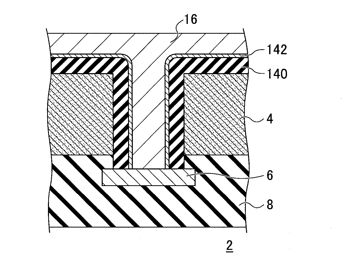
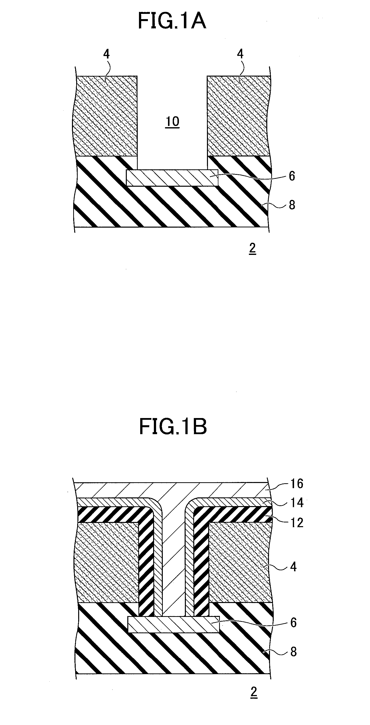
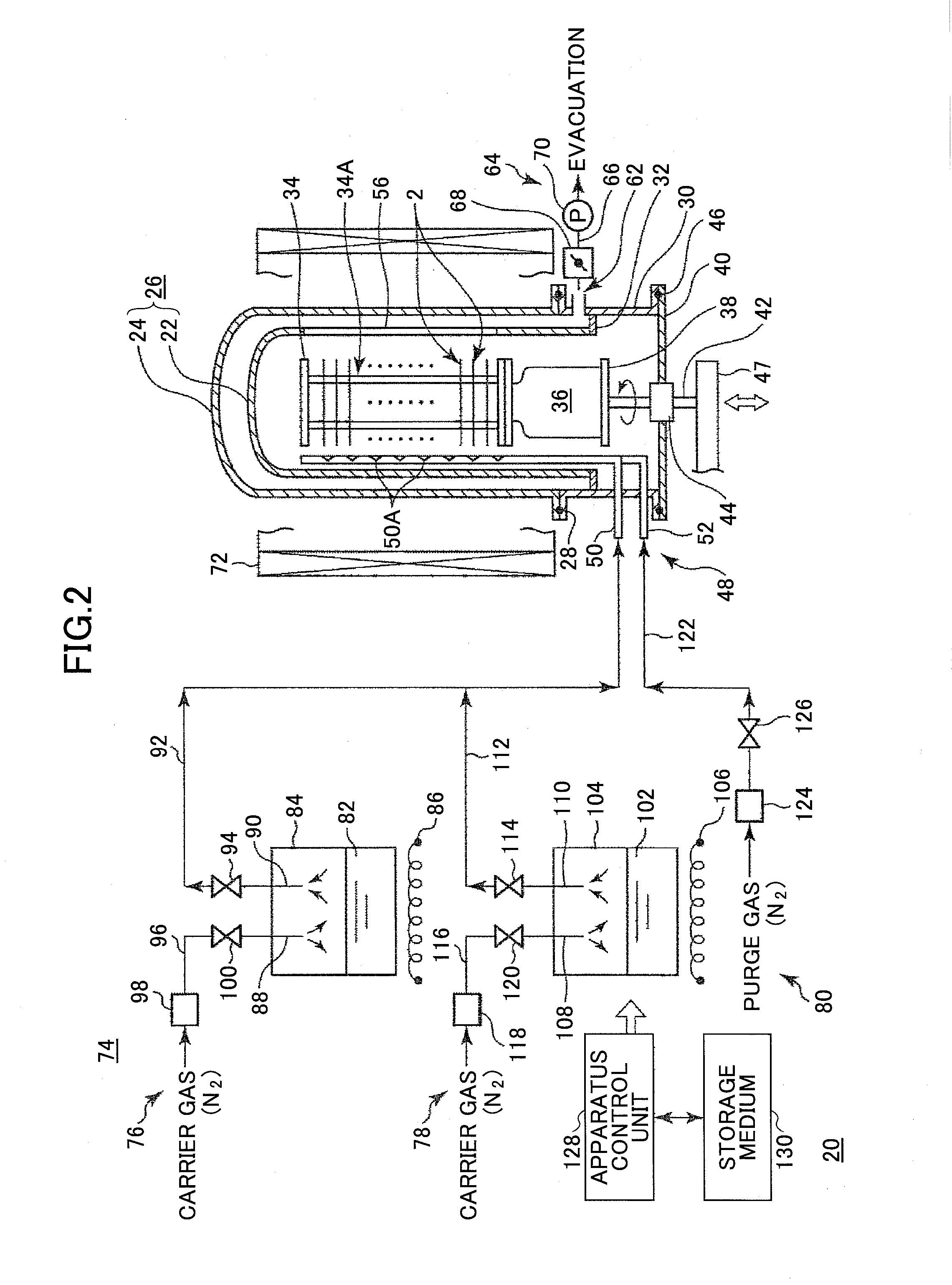
[0033]In the following, embodiments of the present invention are described with reference to the accompanying drawings. FIG. 2 is a vertical cross-sectional configuration diagram illustrating an example of the present invention, and FIG. 3 is a transverse cross-sectional configuration diagram illustrating a film deposition apparatus (heating unit is omitted).

[0034]As illustrated in FIG. 2, the film deposition apparatus 20 includes a process chamber 26 having a double cylindrical structure constituted of an inner cylinder 22 having a cylindrical body with a centroclinal ceiling and an outer cylinder 24 having a cylindrical body with a centroclinal ceiling and arranged outside the inner cylinder 22. The inner cylinder 22 and the outer cylinder 24 are both made of a heat-resistant material, for example, quartz. A lower end of the process chamber 26 is coupled to a manifold 30 having a cylindrical body, for example, made of a stainless steel through a seal member 28 such as an O-ring, a...


PUM

PropertyMeasurementUnit
pressureaaaaaaaaaa
thickaaaaaaaaaa
thicknessaaaaaaaaaa

Abstract

A method for depositing a film is provided. In the method, an object to be processed is accommodated in a process chamber, and an insulating film made of a polymer thin film is deposited on a surface of the object to be processed by supplying a first source gas composed of an acid anhydride and a second source gas composed of a diamine into the process chamber that is evacuated. Next, the insulating film is modified so as to have a barrier function by stopping the supply of the second source gas into the process chamber and continuously supplying the first source gas into the process chamber.

Description

TECHNICAL FIELD[0001]The present invention relates to a method for depositing a film and a film deposition apparatus for depositing an insulating film made of a polymer thin film.BACKGROUND ART[0002]In general, in order to manufacture semiconductor devices, desired devices are manufactured by performing a variety of processes such as a film deposition process, a dry etching process and the like on a substrate such as a semiconductor wafer or the like. However, a line width and a hole diameter are increasingly miniaturized to respond to requirements for further high-integration and fine-miniaturization of semiconductor devices. In fact, in recent years, wire layers have come to have complicated wiring structures such as an eight-layer structure. Furthermore, copper that has low electric resistance and low cost is likely to be used as a wiring material and a filling material because electric resistance needs to be lowered due to the miniaturization of a variety of dimensions (e.g., se...

Claims


Application Information

Patent Timeline
Patent Type & Authority Applications(United States)
IPC IPC(8): H01L21/02C23C16/52C23C16/44C23C16/455
CPCH01L21/02118H01L21/022H01L21/02271C23C16/4408C23C16/455C23C16/52H01L21/02337B05D1/36B05D1/60B05D2490/50H01L21/02359H01L21/76831H01L21/76898
Inventor SUGITA, KIPPEIHASHIMOTO, HIROYUKIHARADA, MUNEO
Owner TOKYO ELECTRON LTD
Why Eureka
Try Eureka