Silver nanostructure-based optical stacks and touch sensors with UV protection

a nanostructure, optical stack technology, applied in the direction of instruments, lighting and heating apparatus, pulse technique, etc., can solve the problems of affecting the application of metal oxide films on flexible substrates, affecting the performance of optical stacks, and prone to damage, etc., to achieve the effect of prolonging the light exposur

Active Publication Date: 2015-04-02
CHAMP GREAT INTL
View PDF2 Cites 18 Cited by
  • Summary
  • Abstract
  • Description
  • Claims
  • Application Information

AI Technical Summary

Benefits of technology

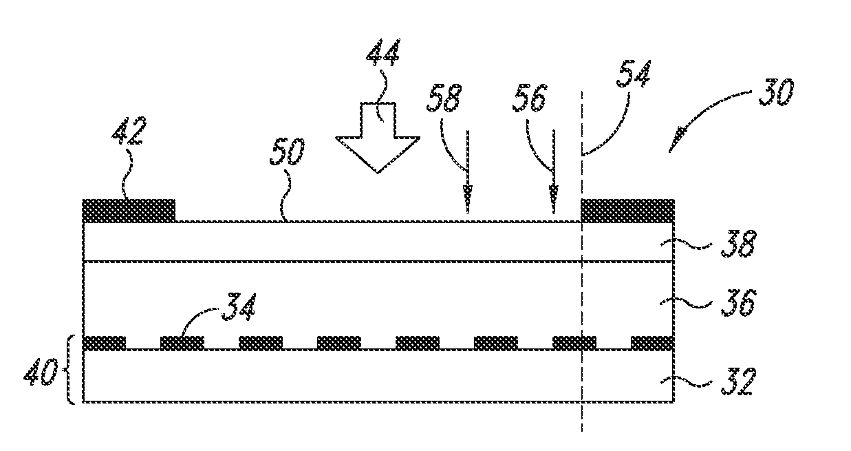
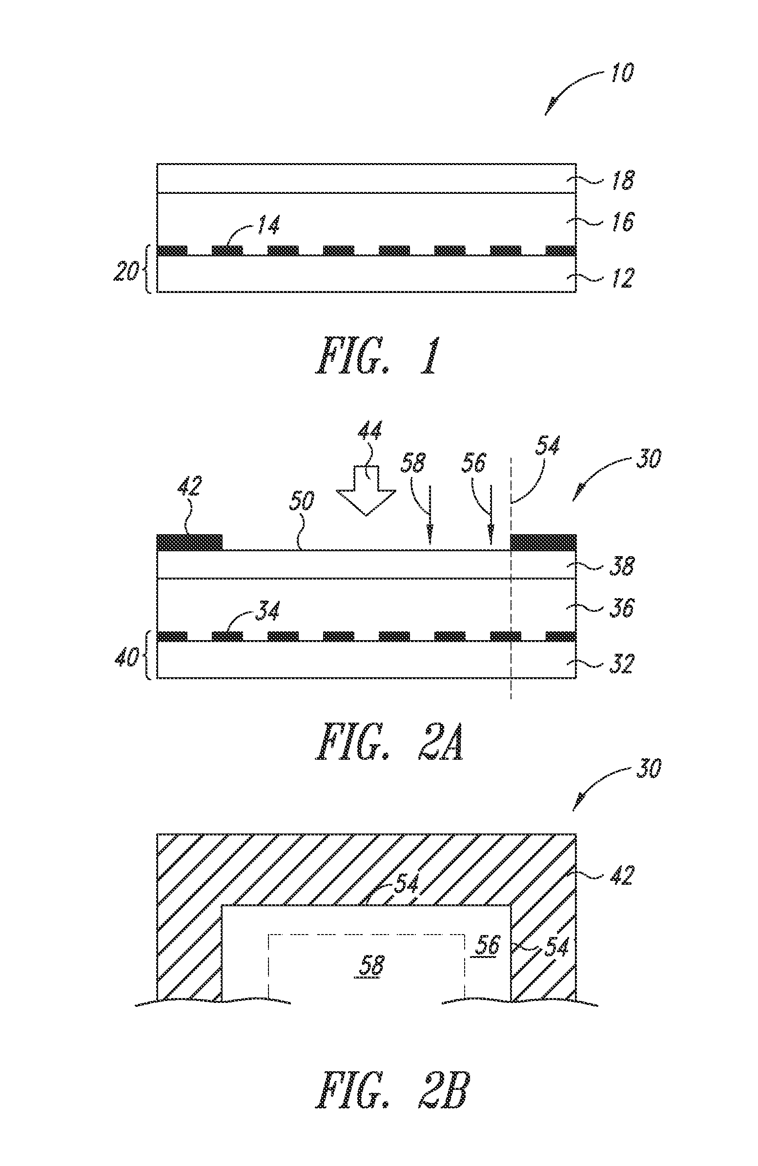
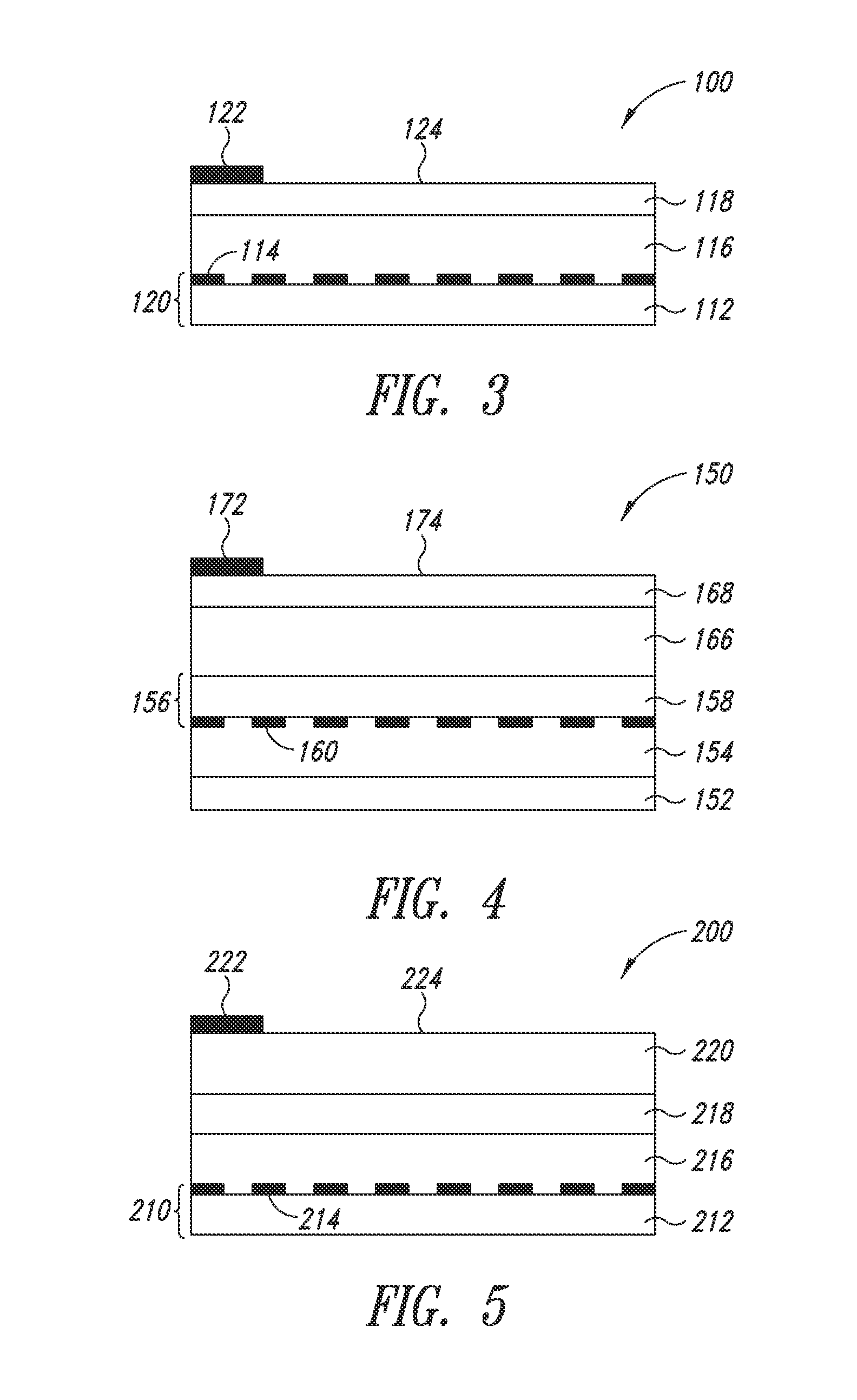
[0010]Disclosed are optical stacks including silver nanostructure-based optical stacks that are stable to prolonged light exposure by incorporating one or more UV-blocking layers.

Problems solved by technology

However, metal oxide films are fragile and prone to damage during bending or other physical stresses.
For certain substrates that are prone to adsorbing moisture, such as plastic and organic substrates (e.g., polycarbonates), it becomes problematic for a metal oxide film to adhere properly.
Applications of metal oxide films on flexible substrates are therefore severely limited.
In addition, vacuum deposition is a costly process and requires specialized equipment.
Moreover, the process of vacuum deposition is not conducive to forming patterns and circuits.
This typically results in the need for expensive patterning processes such as photolithography.
Although generally considered as a noble metal, silver can be sensitive to corrosion under specific circumstances.
One result of silver corrosion is a loss of conductivity either locally or uniformly, which manifests as drifts in sheet resistance of the transparent conductive film, leading to an unreliable performance.

Method used


Image

  • Silver nanostructure-based optical stacks and touch sensors with UV protection
  • Silver nanostructure-based optical stacks and touch sensors with UV protection
  • Silver nanostructure-based optical stacks and touch sensors with UV protection

Examples


example 1

Synthesis of Silver Nanowires

[0099]Silver nanowires were synthesized by the reduction of silver nitrate dissolved in ethylene glycol in the presence of poly(vinyl pyrrolidone) (PVP) following the “polyol” method described in, e.g., Y. Sun, B. Gates, B. Mayers, & Y. Xia, “Crystalline silver nanowires by soft solution processing”, Nanoletters, (2002), 2(2) 165-168. A modified polyol method, described in U.S. Published Application Nos. 2008 / 0210052 and 2011 / 0174190, in the name of Cambrios Technologies Corporation, produces more uniform silver nanowires at higher yields than does the conventional “polyol” method. These applications are incorporated by reference herein in its entirety.

example 2

Standard Film-Fabrication Procedures

[0100]An ink composition was prepared that comprised silver nanowires, a cellulose based binder, and a surfactant (e.g., a fluorosurfactant such as ZONYL® FSA). The ink was slot-die, roll-to-roll coated on a PET film (e.g., MELINEX-454 or TORAY U483) and was allowed to dry to form a nanowire layer. For certain embodiments, a polymeric overcoat was then applied on the nanowire layer.

[0101]The roll-to-roll process can accommodate a variety of substrate and film dimensions. Suitable roll-to-roll deposition processes can include, but are not limited to, slot die, gravure, reverse gravure, micro-gravure, reverse roll and Mayer-bar. More detailed description of the roll-to-roll process can be found in U.S. Pat. No. 8,049,333 and U.S. Published Patent Application No. 2013 / 0040106, in the name of Cambrios Technologies Corporation, the assignee of the present application. Both of these patent documents are incorporated herein by reference in their entireti...

example 3

Light Stability of Films with and without UV-Blocking Layer

[0102]A sample optical stack (1000) without a UV-blocking layer is shown in FIG. 14A. A basic transparent conductive film (1010) having a PET substrate (1020) and a networking layer of silver nanowires (1030) was first made according to Example 2. The basic transparent conductive film was then mounted on a piece of Eagle XG glass (1040) and secured with tapes (1050) around the edges. The nanowires (1030) face the glass (1040) and are loosely in contact with it, but not bonded to it with any adhesive. An air gap (1044) is schematically shown to illustrate this configuration.

[0103]Another sample optical stack (1060) with a UV-blocking layer is shown in FIG. 14B and can be made from the optical stack (1000) of FIG. 14A by laminating a UV-blocking film (1070) on the surface of the glass opposite from the nanowires.

[0104]FIG. 14C shows the transmission spectrum of bare Eagle XG glass, as compared to that of the glass laminated wi...


PUM


Abstract

Disclosed herein are optical stacks that are stable to light exposure by incorporating one or more UV-blocking layers.

Description

CROSS-REFERENCE TO RELATED APPLICATION[0001]This application claims the benefit under 35 U.S.C. §119(e) of U.S. Provisional Patent Application No. 61 / 883,863, filed Sep. 27, 2013, which application is incorporated herein by reference in its entirety.BACKGROUND[0002]1. Technical Field[0003]The disclosure relates to manufacturing stable and reliable optical stacks comprising at least one transparent conductive film of silver nanostructures.[0004]2. Description of the Related Art[0005]Transparent conductors refer to thin conductive films coated on high-transmittance surfaces or substrates. Transparent conductors may be manufactured to have surface conductivity while maintaining reasonable optical transparency. Such surface conducting transparent conductors are widely used as transparent electrodes in flat liquid crystal displays, touch panels, electroluminescent devices, and thin film photovoltaic cells; as anti-static layers; and as electromagnetic wave shielding layers.[0006]Currentl...

Claims


Application Information

Patent Timeline
Patent Type & Authority Applications(United States)
IPC IPC(8): G02B5/20G01R27/00H03K17/96G01R27/26
CPCG02B5/208G01R27/2605H03K2217/96015H03K17/9618H03K2017/9613G01R27/00G06F3/0445
Inventor MANSKY, PAULALLEMAND, PIERRE-MARC
Owner CHAMP GREAT INTL
Why Eureka
Try Eureka