Fabrication method of silicon carbide semiconductor element

a technology of silicon carbide and semiconductor elements, which is applied in the direction of polycrystalline material growth, crystal growth process, chemically reactive gas, etc., can solve the problem that the performance of vertical power device semiconductor elements cannot be realized, and achieve the effect of reducing the size of an elemen

Active Publication Date: 2015-04-23
FUJI ELECTRIC CO LTD
View PDF4 Cites 3 Cited by
  • Summary
  • Abstract
  • Description
  • Claims
  • Application Information

AI Technical Summary

Benefits of technology

[0026]The fabrication method of a silicon carbide semiconductor element according to the present invention produces an effect that enables reductions in the size of an element.

Problems solved by technology

Since 3C—SiC does not have a sufficiently high material physical property as compared to 4H—SiC, the element performance expected of vertical power device semiconductor elements cannot be realized.

Method used


Image

  • Fabrication method of silicon carbide semiconductor element
  • Fabrication method of silicon carbide semiconductor element
  • Fabrication method of silicon carbide semiconductor element

Examples


first embodiment

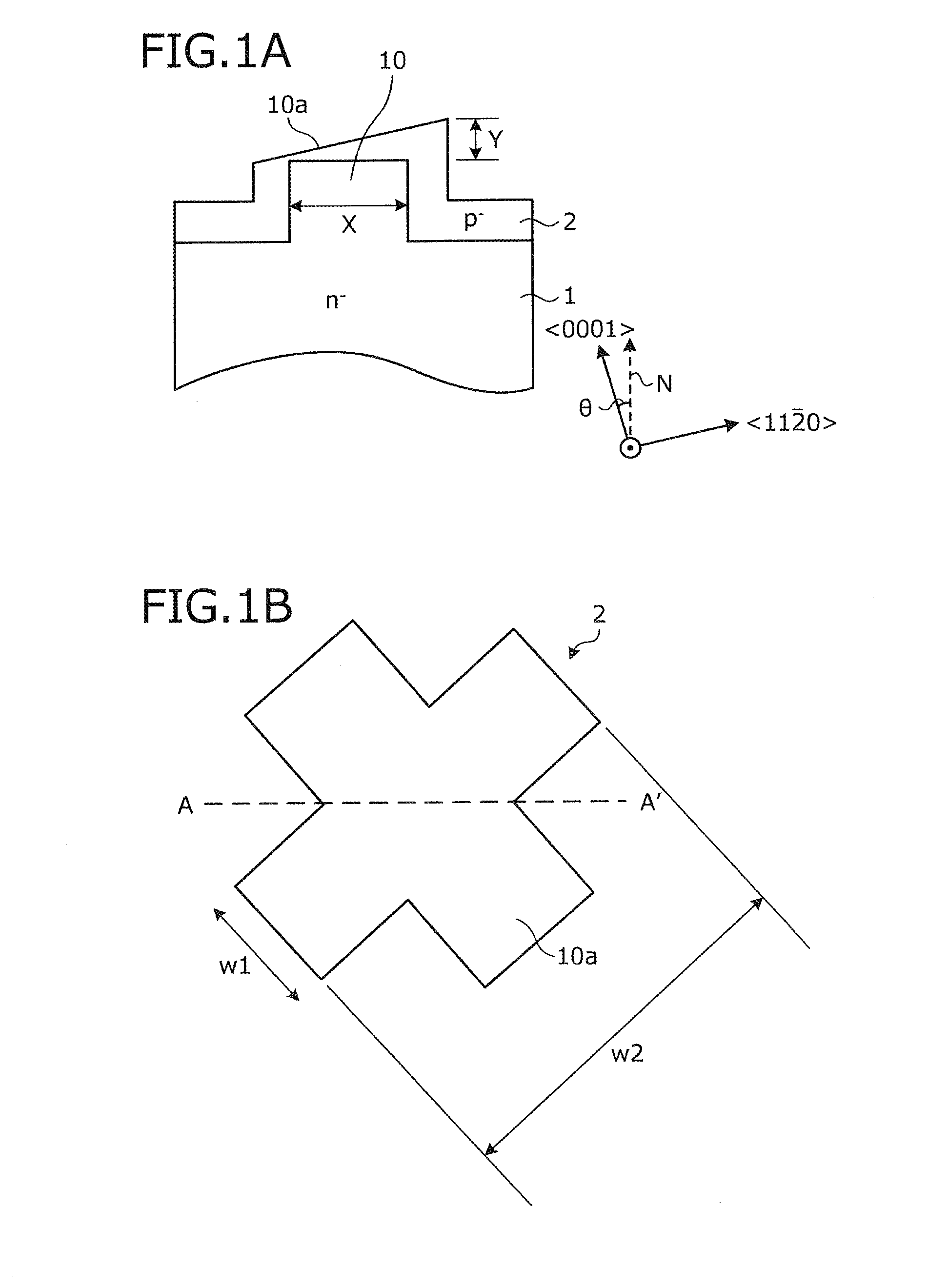
[0035]A fabrication method of a silicon carbide semiconductor element according to a first embodiment of the present invention will be described. FIG. 1 is an explanatory view of a state during fabrication of silicon carbide semiconductor element according to the first embodiment of the present invention. FIG. 1(a) is a cross-sectional view of main components, taken along a cut line A-A′ of FIG. 1(b), and depicts a state of an alignment mark 10 after formation of a p type epitaxial layer 2. FIG. 1(b) is a plane view of a plane shape of the alignment mark 10.

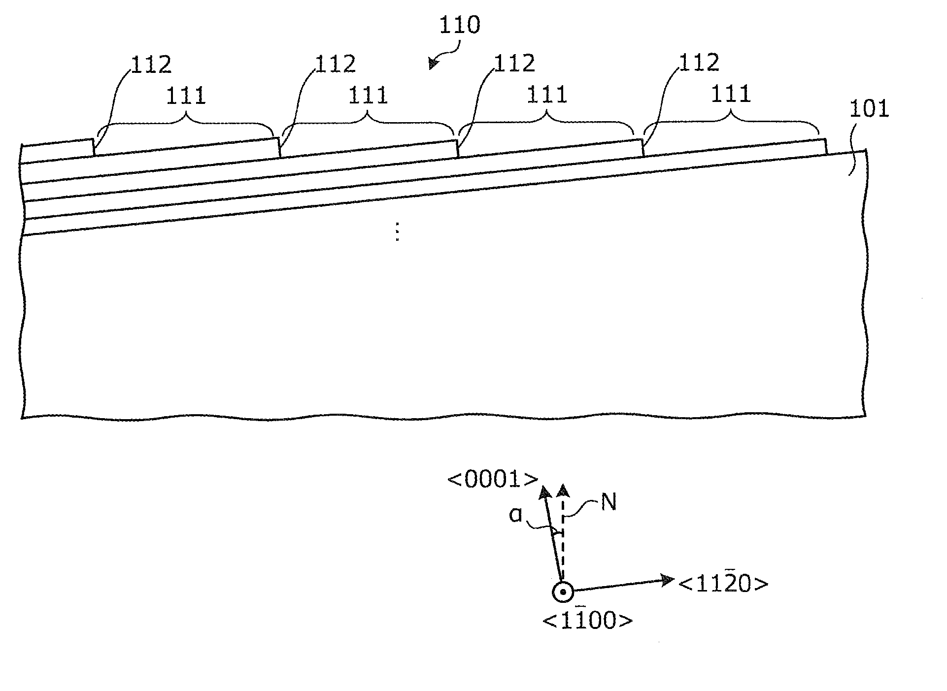
[0036]First, an n− type silicon carbide monocrystal substrate (hereinafter referred to as an n− type silicon carbide substrate) 1 is prepared that includes four-layer cycle hexagonal crystals of silicon carbide (4H—SiC), with an n− type silicon carbide epitaxial layer on one principal surface, for example. The principal plane of the n− type silicon carbide substrate 1 is a (000-1) C-plane having an off-angle θ in a direction. Fo...

second embodiment

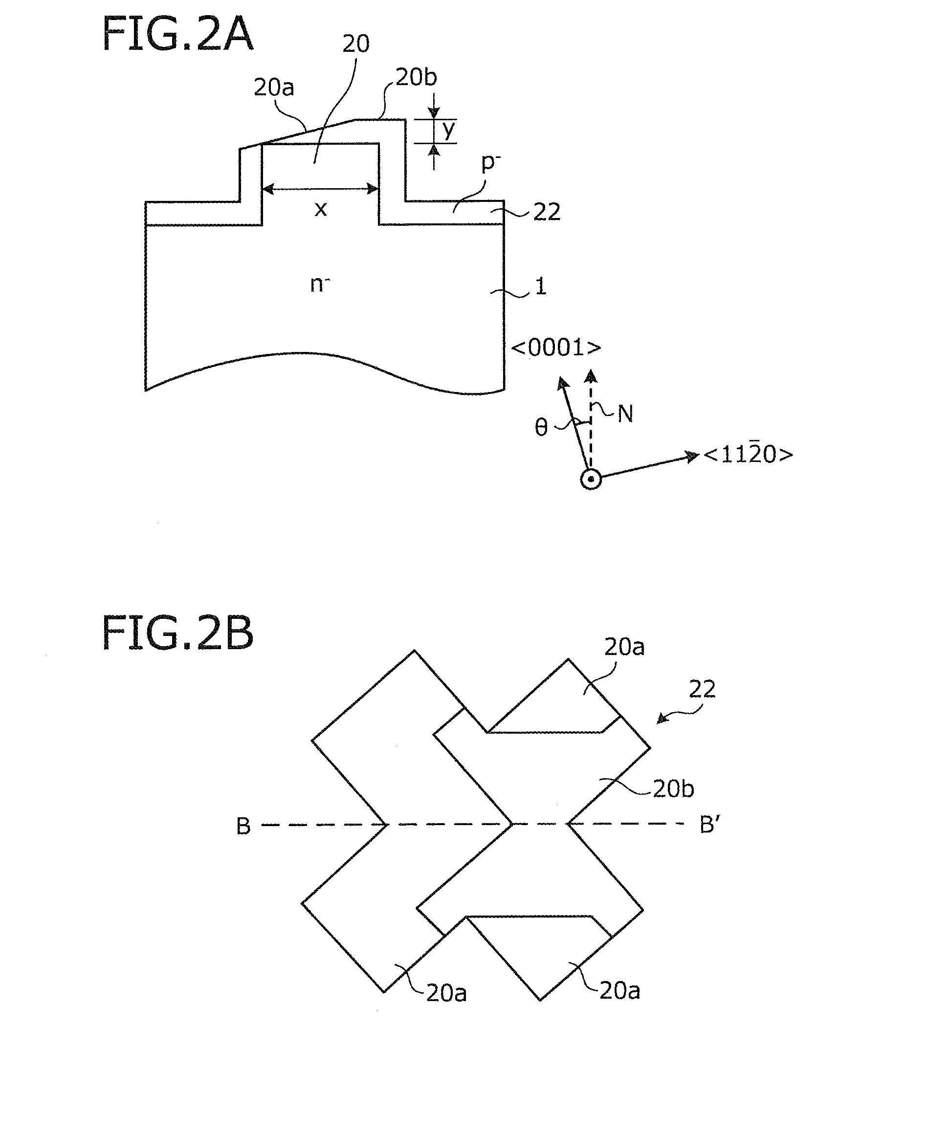
[0045]The fabrication method of a silicon carbide semiconductor element according to a second embodiment will be described. The fabrication method of a silicon carbide semiconductor element according to the second embodiment is different from the fabrication method of a silicon carbide semiconductor element according to the first embodiment in that a silicon carbide epitaxial layer grown convexly into a cross-like plane shape on a principal surface of an n− type silicon carbide substrate is defined as an alignment mark. For example, in the fabrication method of a silicon carbide semiconductor element according to the second embodiment, the alignment mark is formed as follows.

[0046]First, as is the case with the first embodiment, an n− type silicon carbide substrate is prepared that has an n− type silicon carbide epitaxial layer on one principal surface. For example, a tantalum carbide (TaC) film is formed on the principal surface of the n− type silicon carbide substrate on the n− ty...

third embodiment

[0052]The fabrication method of a silicon carbide semiconductor element according to a third embodiment will be described. The fabrication method of a silicon carbide semiconductor element according to the third embodiment is different from the fabrication method of a silicon carbide semiconductor element according to the first embodiment in that an alignment mark recessed in a concaved shape from the principle surface of the n− type silicon carbide substrate is formed and that a region including the alignment mark is coated with a tantalum carbide film. For example, in the fabrication method of a silicon carbide semiconductor element according to the third embodiment, the alignment mark is formed as follows.

[0053]In the third embodiment, first, as is the case with the first embodiment, a mask oxide film deposited on the principal surface of the n− type silicon carbide substrate is patterned by photolithography and etching. In the third embodiment, the mask oxide film is formed with...


PUM

PropertyMeasurementUnit
depthaaaaaaaaaa
thicknessaaaaaaaaaa
thicknessaaaaaaaaaa

Abstract

A (000-1) C-plane of an n− type silicon carbide substrate having an off-angle θ in a <11-20> direction is defined as a principal plane, and a periphery of a portion of this principal surface layer defined as an alignment mark is selectively removed to leave the convex-shaped alignment mark. The alignment mark has a cross-like plane shape such that two rectangles having longitudinal dimensions tilted by 45 degrees relative to the <11-20> direction are orthogonal to each other. When a film thickness of a p− type epitaxial layer is Y; a width of the alignment mark parallel to the principal surface of the n− type silicon carbide substrate is X; and an off-angle of the n− type silicon carbide substrate is θ, an epitaxial layer is formed on an upper surface of the alignment mark such that Y≧X·tan θ is satisfied.

Description

TECHNICAL FIELD[0001]The present invention relates to a fabrication method of a silicon carbide semiconductor element using silicon carbide (SiC) as a semiconductor material, particularly, to which current is applied from a front surface side to a back surface side of a semiconductor substrate.BACKGROUND ART[0002]A silicon carbide semiconductor has a large band gap as compared to a silicon (Si) semiconductor and therefore, has high dielectric breakdown electric field intensity. ON-resistance is resistance in a conductive state and is inversely proportional to the cube of the dielectric breakdown electric field intensity and therefore, for example, widely used silicon carbide semiconductors called a 4H type (four-layer cycle hexagonal crystals: 4H—SiC) can suppress the ON-resistance to a few hundredth as compared to silicon semiconductors.[0003]Therefore, also because of large thermal conductivity characteristics facilitating heat radiation, silicon carbide semiconductors are expecte...

Claims


Application Information

Patent Timeline
Patent Type & Authority Applications(United States)
IPC IPC(8): H01L21/02H01L23/544
CPCH01L21/02378H01L23/544H01L21/02609H01L21/02491C30B25/186C30B25/20C30B29/36H01L21/0243H01L21/02433H01L21/02529H01L29/045H01L29/1608H01L29/861H01L29/872H01L2223/5442H01L2223/54426H01L2223/5446H01L2924/0002
Inventor TSUJI, TAKASHIFUKUDA, KENJI
Owner FUJI ELECTRIC CO LTD
Why Eureka
Try Eureka