

Integrated contactless signal transfer apparatus
- Summary
- Abstract
- Description
- Claims
- Application Information
AI Technical Summary
Benefits of technology
Problems solved by technology
Method used
Image

Examples
Embodiment Construction
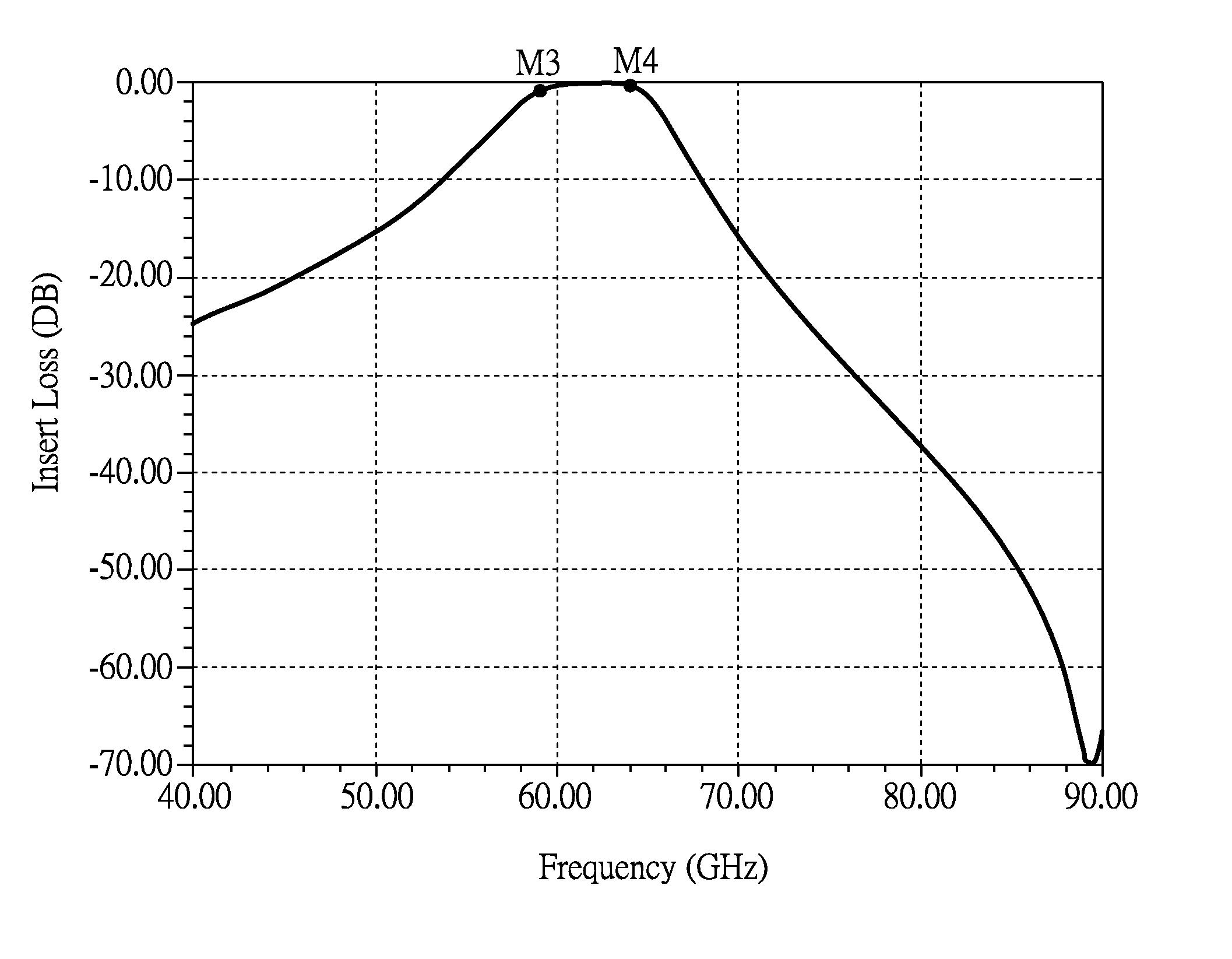
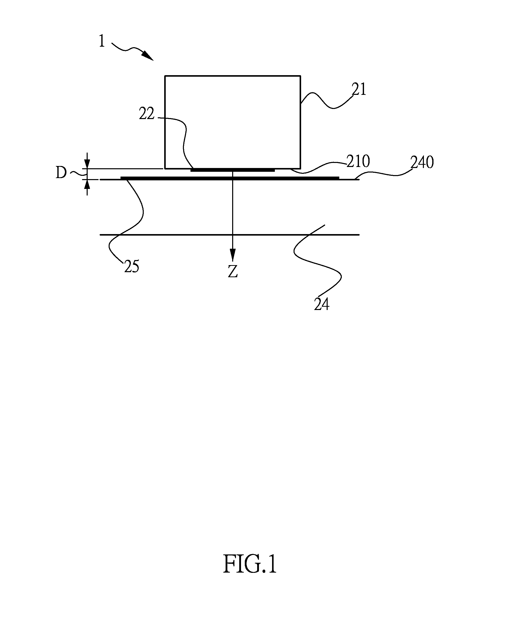
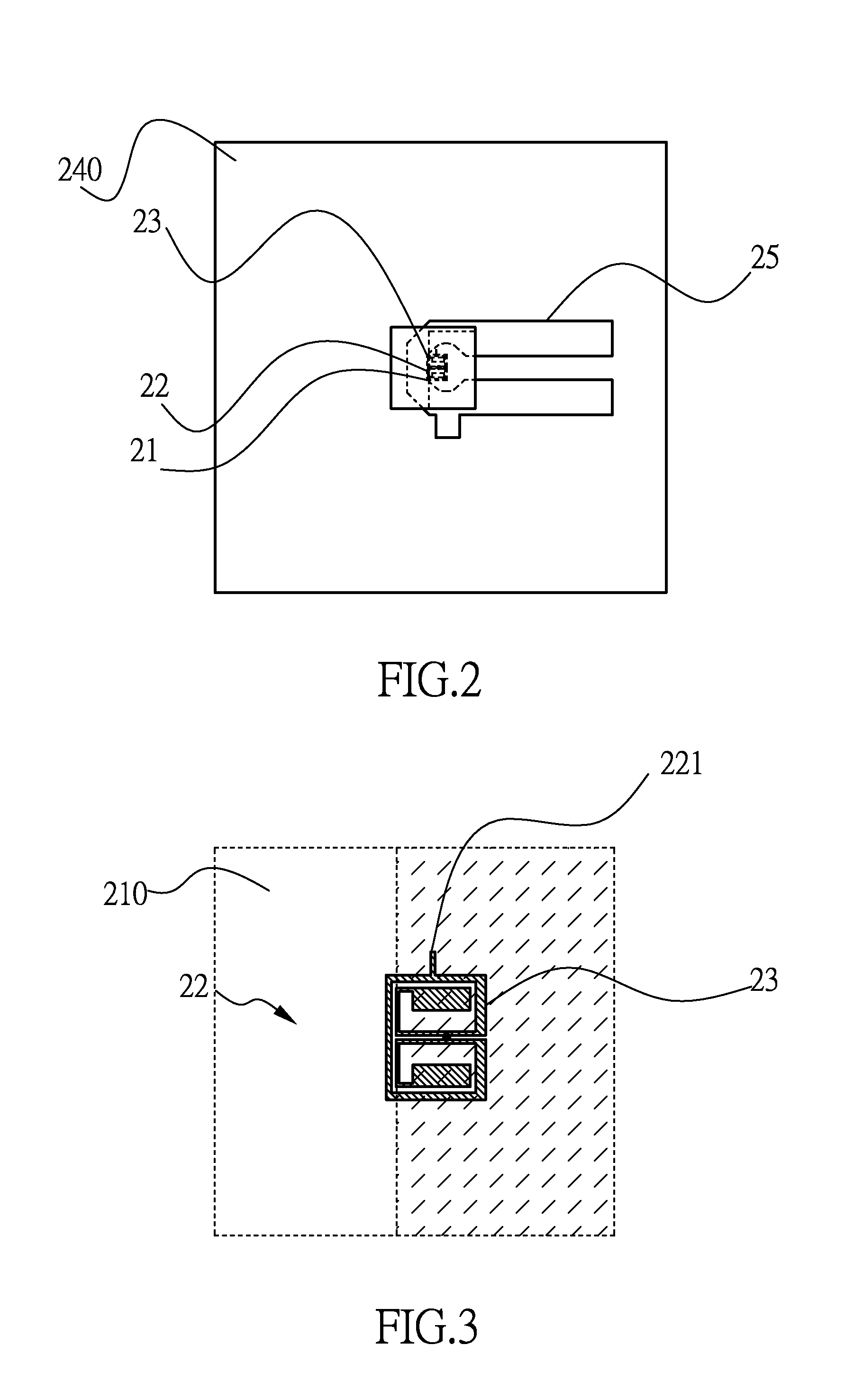
[0030]FIG. 1 is a schematic diagram of an integrated contactless signal transfer apparatus according to a preferred embodiment of the invention, and FIG. 2 is a top view of an integrated contactless signal transfer apparatus according to a preferred embodiment of the invention. With reference to FIG. 1 (along a Z axis) and FIG. 2, the integrated contactless signal transfer apparatus I includes a substrate 21, a chip 22, a first resonator unit 23, a PCB 24, and a second resonator unit 25. The substrate 21 has a first surface 210. The chip 22 is disposed on the first surface 210. The first resonator unit 23 is disposed on the chip 22 to receive a first signal (not shown) with a first frequency generated from the chip 22. The PCB 24 has a second surface opposite to the first surface 210 and is disposed to have a gap D between the substrate 21 and the PCB. Namely, the gap D is a distance from the first surface 210 to the second surface 240. Thus, the PCB 24 is kept to have no physical t...
PUM
 Abstract
Description
Claims
Application Information