Method of manufacturing structures of leds or solar cells

a technology of leds and solar cells, applied in the manufacture of final products, basic electric elements, solid-state devices, etc., can solve the problems of reducing the manufacturing yield of the structure in question, limiting the choice of materials that can form the substrate, and being expensive and relatively unavailable on the material market. , to achieve the effect of improving the quality of bonding

Active Publication Date: 2015-04-30
S O I TEC SILICON ON INSULATOR THECHNOLOGIES
View PDF7 Cites 29 Cited by
  • Summary
  • Abstract
  • Description
  • Claims
  • Application Information

AI Technical Summary

Benefits of technology

[0031]Obtaining such a surface quality in advance makes it possible to then carry out bonding by molecular adhesion under favorable conditions.
[0032]The method can further comprise, between steps d) and e), a step of annealing at a temperature less than or equal to 100° C. This annealing makes it possible to substantially improve the quality of the bonding by molecular adhesion.

Problems solved by technology

The Applicant has, however, observed several major disadvantages related to the thermocompression bonding technique.
A CTE mismatch that is too great is likely to lead to fractures and, consequently, to reduce the manufacturing yields of the structures in question.
These CTE compatibility constraints considerably limit the choice of materials that can form substrates 2 and 8.
The choice can, for example, be concerned with germanium, which has the disadvantage, however, of being expensive and relatively unavailable on the materials market.

Method used


Image

  • Method of manufacturing structures of leds or solar cells
  • Method of manufacturing structures of leds or solar cells
  • Method of manufacturing structures of leds or solar cells

Examples


first embodiment

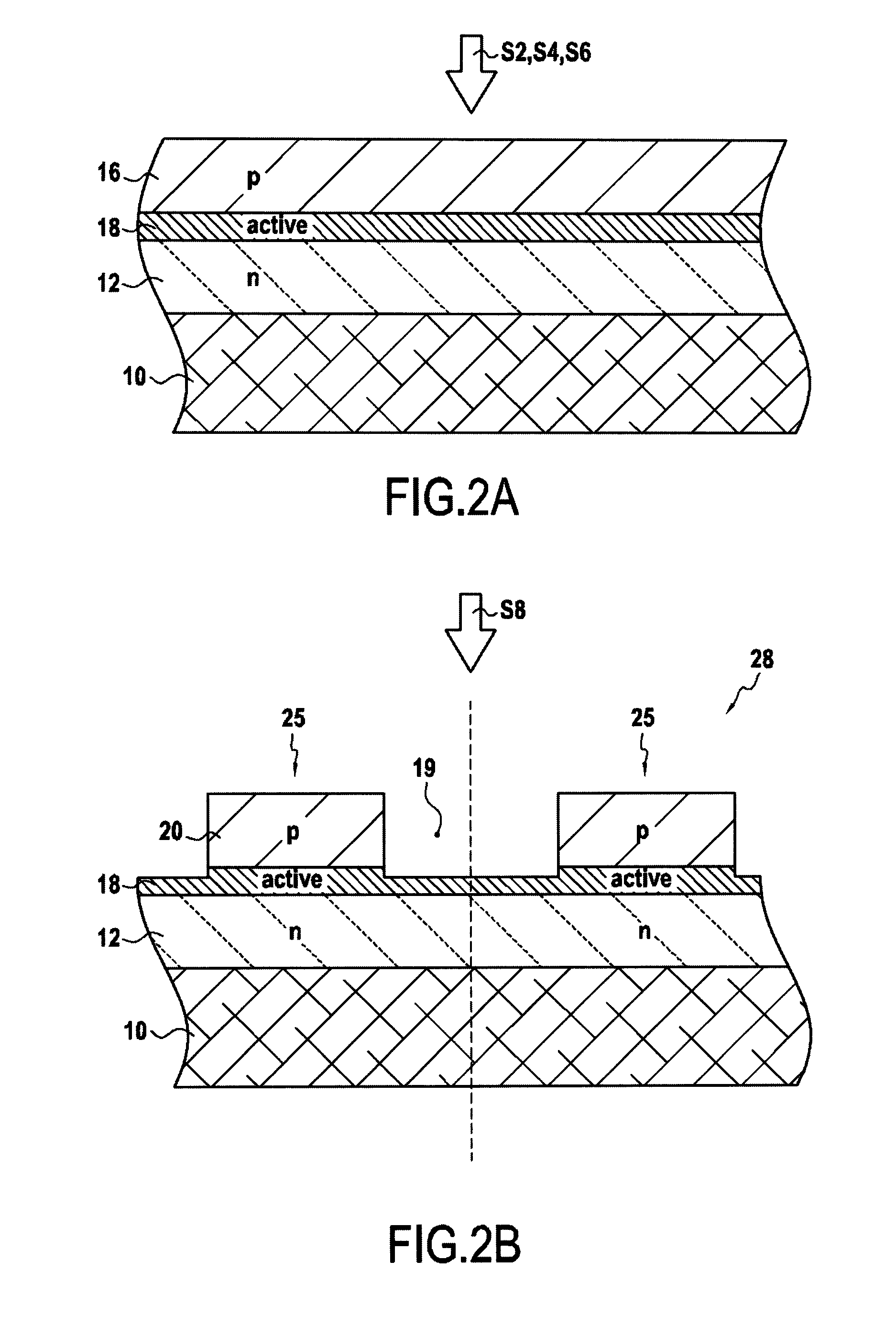
[0045]A method of manufacturing LED devices in accordance with the disclosure is now described in reference to FIGS. 2A to 2I and 3.

[0046]In a first embodiment, the method is implemented from a plate or support substrate 10. The support substrate 10 is sapphire in this example, other materials, however, being possible, notably such as silicon, silicon carbide or germanium.

[0047]An n-type layer 12 (about 1 or 2μm in thickness), an active layer 14 (about 10 nm) and a p-type layer 16 (between about 100 nm and 200 nm in thickness) are first deposited successively by epitaxy on the support substrate (10) (respectively, S2, S4 and S6, FIG. 2A). The manner in which these layers are prepared is known to the person skilled in the art and, thus, will not be described in further detail in this document.

[0048]The n- and p-type layers can be formed in the reverse order and can include several sub-layers of different compositions, thicknesses or dopant concentrations, comprising unintentionally d...

second embodiment

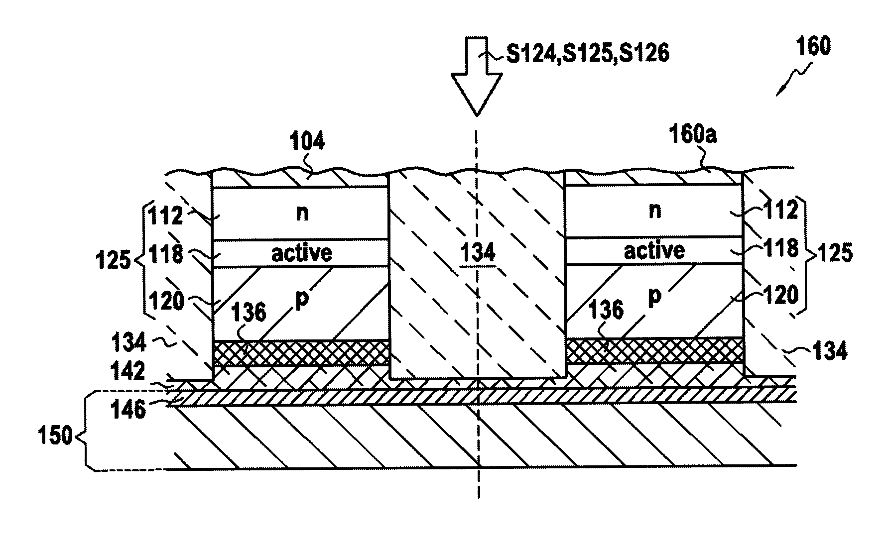
[0094]FIGS. 4A to 4I and 5 represent the manufacture of LED devices in accordance with the disclosure.

[0095]This second embodiment is on the whole very similar to the first embodiment described above in reference to FIGS. 2A-2I and 3.

[0096]This second embodiment differs from the first in that the elemental LED structures (here noted 125) are formed on a composite growth substrate 100, the latter comprising a support substrate 110, a buried layer 102 and growth islands 104 (FIGS. 2A and 2B).

[0097]The support substrate (here 101) consists of sapphire. Substrate 110 can also be composed of a semiconductor material, notably, such as silicon, silicon carbide or germanium. The buried layer 102 is an adaptation layer prepared here in SiO2. The growth islands 104 are obtained from a growth layer of relaxed material, here a layer of InGaN prepared, for example, by epitaxial growth on a seed layer of GaN and then transferred onto the support substrate 110 via the buried layer 102.

[0098]Trench...


PUM

PropertyMeasurementUnit
surface roughnessaaaaaaaaaa
temperatureaaaaaaaaaa

Abstract

The invention disclosure relates to a manufacturing method comprising the formation of elemental LED or photovoltaic structures on a first substrate, each comprising at least one p-type layer, an active zone and an n-type layer, formation of a first planar metal layer on the elemental structures, provision of a transfer substrate comprising a second planar metal layer, assembly of the elemental structures with the transfer substrate by bonding of the first and second metal layers by molecular adhesion at room temperature, and removal of the first substrate.

Description

CROSS-REFERENCE TO RELATED APPLICATIONS[0001]This application is a national phase entry under 35 U.S.C. § 371 of International Patent Application PCT / EP2013 / 062423, filed Jun. 14, 2013, designating the United States of America and published in English as International Patent Publication WO 2013 / 189857 A1 on Dec. 27, 2013, which claims the benefit under Article 8 of the Patent Cooperation Treaty and under 35 U.S.C. § 119(e) to French Patent Application Ser. No. 1257617, filed Aug. 6, 2012, French Patent Application Ser. No. 1255931, filed Jun. 22, 2012, and French Patent Application Ser. No. 1255934, filed Jun. 22, 2012, the disclosure of each of which is hereby incorporated herein in its entirety by this reference.TECHNICAL FIELD[0002]The disclosure relates to the manufacture of light-emitting diodes (LEDs) and those of solar (photovoltaic) cells.BACKGROUND[0003]LEDs are generally manufactured from elemental structures corresponding to a stack of layers comprising at least one n-typ...

Claims


Application Information

Patent Timeline
Patent Type & Authority Applications(United States)
IPC IPC(8): H01L33/32H01L27/15H01L31/0304H01L27/142H01L33/00H01L31/18
CPCH01L33/32H01L33/0075H01L33/0079H01L27/153H01L31/1844H01L31/03044H01L27/142H01L31/1892H01L27/156H01L31/02008H01L31/075H01L33/007H01L33/20H01L33/44H01L2933/0016H01L33/0093H01L2224/24137H01L2224/32225H01L2224/73267H01L2224/82H01L2224/92244H01L2924/3512Y02E10/52Y02E10/544Y02E10/548Y02P70/50H01L21/187H01L21/2007H01L33/385H01L25/042H01L25/0753H01L31/03048H01L31/035236H01L31/055H01L31/1848H01L31/1852H01L31/1864H01L33/0095H01L33/06H01L33/12H01L33/46H01L33/502H01L33/58H01L33/62H01L2224/18H01L31/0543H01L31/056
Inventor GUENARD, PASCAL
Owner S O I TEC SILICON ON INSULATOR THECHNOLOGIES
Why Eureka
Try Eureka