Method and Hardware for Enhanced Removal of Post Etch Polymer and Hardmask Removal

a post-etch polymer and hardmask technology, applied in the field of semiconductor processing, can solve the problems of high cost, high cost, and high cost of polymer layer thickening, so as to reduce the trench aspect ratio, reduce the risk of pattern collapse, and increase the cost

Active Publication Date: 2015-05-14
TOKYO ELECTRON LTD
View PDF3 Cites 40 Cited by
  • Summary
  • Abstract
  • Description
  • Claims
  • Application Information

AI Technical Summary

Benefits of technology

[0006]A given etch process is a balance of deposition, diffusion, chemisorption, surface and gas phase reactions between reactant species and the substrate. Polymer thickness can also be controlled by changing the plasma tool process parameter such as bias voltage, gas composition, pressure etc. By way of an example substrate composition of Si / SiO2, there are various surface kinetics in play during etching of such a substrate. Fluorocarbon etching of SiO2 relies on polymerization and chemically enhanced sputtering. CxFy passivation can regulate delivery of precursors and activation energy. Chemisorption of CFx can produce a complex at the oxide-polymer interface (oxide underneath a polymer top layer). Etch precursors and products can diffuse through the polymer layer. In some substrate stacks this diffusion can consume the polymer. In silicon etching, however, CFx may not be consumed, resulting in thicker polymer layers.
[0009]An additional challenge for post-etch cleans is a further requirement to remove the hardmask used in the corresponding etch process that contributes to polymer deposition. It is desirable to remove hardmasks during a wet clean to reduce the aspect ratio of the trenches and reduce a risk of pattern collapse during the drying process, which can also eliminate a need for hardmask removal in a chemical-mechanical polishing (CMP) step after a copper fill step. CMP processes are more expensive than wet clean processes and are also more abrasive which can damage structures.
[0010]Systems and methods herein include an ultraviolet (UV) light exposure in a wet spin chamber that can operate under atmospheric pressure. The performance of conventional wet chemicals used in fabrication can be enhanced by customized selection of an electromagnetic radiation source. Techniques herein reduce thermal budgets and / or process times by increasing or expanding the reactivity of the vapor or liquid chemistry used in a cleaning process. Processes include sequential removal of a polymer film followed by removal of a metal hard mask. Alternative processes include simultaneous removal of polymer film and metal hard mask.
[0012]Accordingly, the polymer film and hardmask layer can both be cleaned from the substrate. Techniques herein have been demonstrated to increase the strip rate of a TiN hardmask film by 100% as compared to conventional techniques of stripping TiN hardmasks. Conventionally, hardmasks are removed from low-k films using a wet etching process in which a solution containing hydrogen peroxide (H2O2) is dispensed on a spinning wafer at an elevated temperature. The H2O2 reacts with the hardmask to dissolve the hardmask, leaving underlying films and structures on the substrate. The drawback of such a cleaning process is that conventionally this process treats a single wafer at a time, and cleaning a given TiN hardmask from a wafer (such as a 300 mm diameter) can take about 6 minutes. Such a relatively long treatment time reduces throughput and efficiency. Thus, the improvements herein are advantageous in improving productivity of the post etch cleaning tool, by reducing a treatment temperature of TiN strip chemistry, reducing an amount of chemistry used, and extending lifetime of a strip tool and chemistry, and enabling the polymer films to be removed including such polymer films that would otherwise not be removable using conventional wet cleaning chemistry.

Problems solved by technology

Such dielectric films can be porous and susceptible to damage.
In some substrate stacks this diffusion can consume the polymer.
In silicon etching, however, CFx may not be consumed, resulting in thicker polymer layers.
In fabrication facilities around the world, integrated circuit makers are increasingly finding post-etch polymers that are difficult to remove or that cannot be removed with conventional chemicals or ash processes without damaging the sensitive low-k dielectric layer below.
An additional challenge for post-etch cleans is a further requirement to remove the hardmask used in the corresponding etch process that contributes to polymer deposition.
CMP processes are more expensive than wet clean processes and are also more abrasive which can damage structures.
The drawback of such a cleaning process is that conventionally this process treats a single wafer at a time, and cleaning a given TiN hardmask from a wafer (such as a 300 mm diameter) can take about 6 minutes.
Such a relatively long treatment time reduces throughput and efficiency.

Method used


Image

  • Method and Hardware for Enhanced Removal of Post Etch Polymer and Hardmask Removal
  • Method and Hardware for Enhanced Removal of Post Etch Polymer and Hardmask Removal
  • Method and Hardware for Enhanced Removal of Post Etch Polymer and Hardmask Removal

Examples


Embodiment Construction

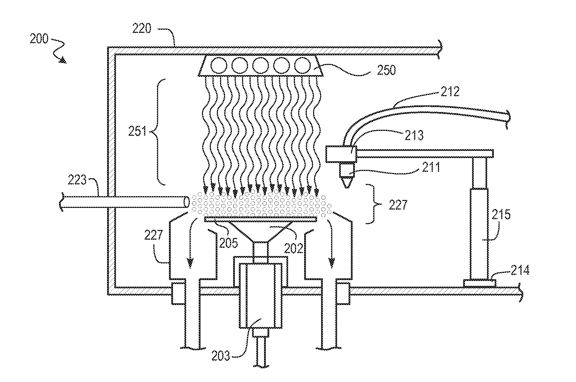
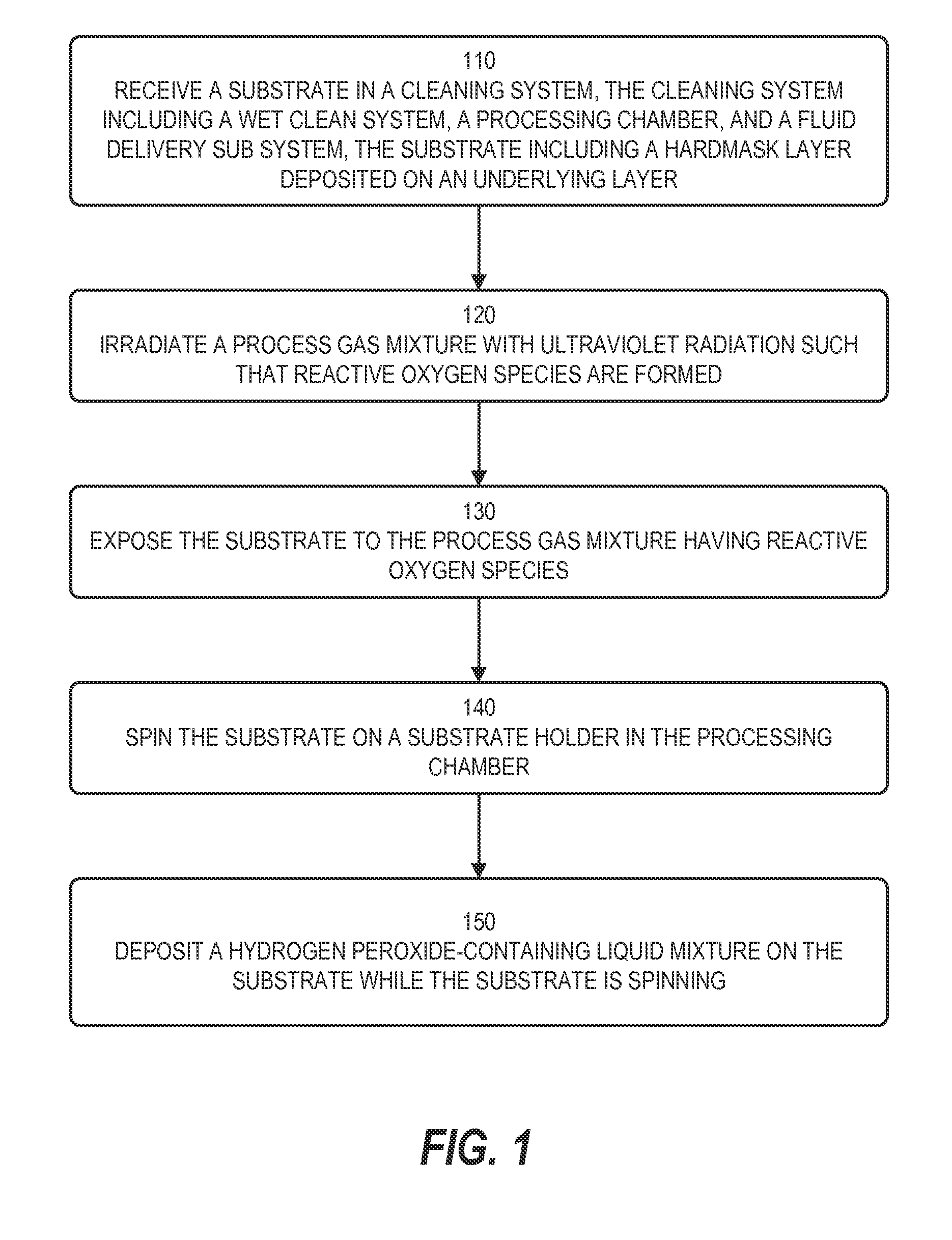
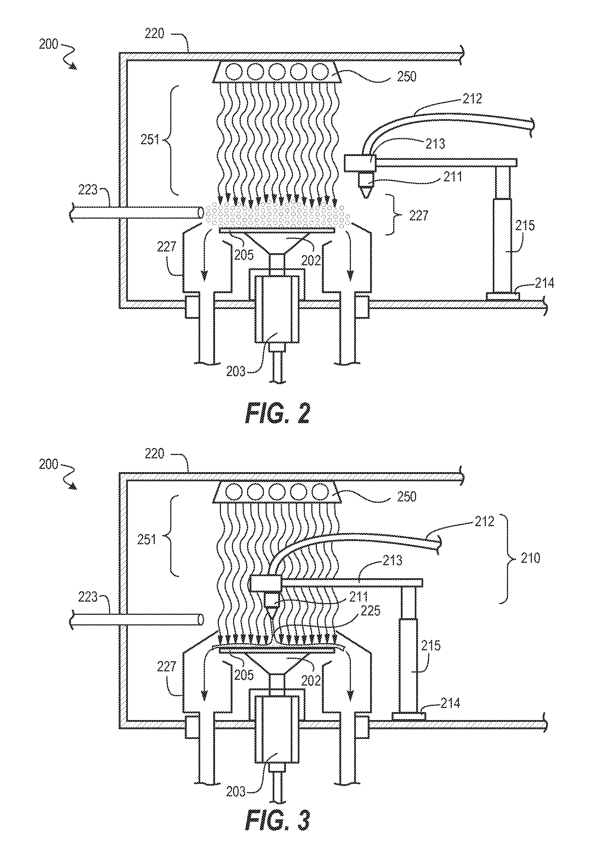
[0021]Techniques herein include methods for using an ultraviolet (UV) light exposure wet spin chamber that can operate under atmospheric pressure. At least two process modes can be selected for use. In a first process mode, a substrate is exposed to electromagnetic radiation. The substrate is dry with no liquid on the surface of the substrate. The substrate can be stationary or spinning. The atmosphere can be of several options. The atmosphere can be oxidizing (air, clean dry air, oxygen, low oxygen atmosphere (greater than 0.1 ppm but less than 21%) or peroxide vapor, peracetic acid vapor, acetic acid vapor or other volatile peroxygen compound. The atmosphere can be a reducing environment (hydrogen-containing atmosphere below the lower explosive limit, ammonia environment below the lower explosive limit. The atmosphere can be a combination of oxidizer and reducing gases. Alternatively, the atmosphere can be inert gas ambient. For safety the concentration of each component should be...


PUM


Abstract

Methods for cleaning substrates are described including cleaning substrates having hardmask masks and polymer films, such part of semiconductor fabrication. Cleaning methods include ultraviolet (UV) light exposure of process gas mixtures and liquid cleaning chemistries. A substrate and / or process fluids are exposed to ultraviolet radiation. A process gas mixture being irradiated can include an oxidizing gas mixture (air, clean dry air, oxygen, peroxygen, etc.). Reducing gas mixtures, having hydrogen, can also be irradiated. Reactive species from irradiated gas mixtures are exposed to the substrate to chemically modify film properties, such as by facilitating a subsequent liquid cleaning step. Liquid cleaning chemistries on a substrate surface can also be irradiated. Such cleaning techniques enable shorter cleaning times, lower processing temperatures, and reduced damage to underlying or intermediate layers such as dielectric layers.

Description

CROSS REFERENCE TO RELATED APPLICATIONS[0001]The present application claims the benefit of U.S. Provisional Patent Application No. 61 / 902,485, filed on Nov. 11, 2013, entitled “Method and Hardware for Enhanced Removal of Post Etch Polymer and Hardmask Removal,” which is incorporated herein by reference in its entirety.BACKGROUND OF THE INVENTION[0002]The present application relates generally to semiconductor processing and relates particularly to a substrate cleaning processes.[0003]Fabrication of integrated circuits and semiconductor devices can involve many different types of processing techniques. Such techniques generally involve patterning a substrate and using the pattern to make various sacrificial and / or permanent structures. For example, photolithography can be used to create patterned layers using a thin layer of radiation-sensitive material, such as photoresist. This radiation-sensitive layer is transformed into a patterned mask that can be used to etch or transfer a patt...

Claims


Application Information

Patent Timeline
Patent Type & Authority Applications(United States)
IPC IPC(8): H01L21/311
CPCH01L21/31133H01L21/02063H01L21/31111H01L21/31144H01L21/32134H01L21/67051H01L21/67115H01L21/02041
Inventor BROWN, IAN J.LIU, JUNJUN
Owner TOKYO ELECTRON LTD
Why Eureka
Try Eureka