Multilayered wiring substrate

a wiring substrate and multi-layer technology, applied in the direction of conductors, fixed capacitor details, printed circuit non-printed electric components association, etc., can solve the problems of circuit malfunction, transmission loss of high-frequency signals, difficulty in directly connecting the ic chip on the motherboard, etc., to achieve low cost, high electrical conductivity, and easy formation of conductor layers

Inactive Publication Date: 2015-05-21
NGK SPARK PLUG CO LTD
View PDF52 Cites 4 Cited by
  • Summary
  • Abstract
  • Description
  • Claims
  • Application Information

AI Technical Summary

Benefits of technology

[0023]The conductor layers can be formed of an electrically conductive metal material. Examples of a metal material used to form the conductor layers include copper, silver, iron, cobalt, and nickel. Particularly, the conductor layers are formed preferably of copper, which is high in electrical conductivity and is inexpensive. Also, preferably, the conductor layers are formed by plating. By doing so, the conductor layers can be formed with ease and at low cost. However, the conductor layers may be formed through application of metal paste by printing.
[0024]The via conductor connected to at least the main-surface-side electrode layer is provided in the interlayer insulating layers of the wiring laminate formed on at least the core main-surface. For example, the multilayer wiring substrate comprises, as the via conductor, one or a plurality of main-surface-side via conductors provided in the interlayer insulating layers of the wiring laminate on the core main-surface and connected to the main-surface-side electrode layer, and one or a plurality of back-surface-side via conductors provided in the interlayer insulating layers of the wiring laminate on the core back-surface and connected to the back-surface-side electrode layer. In this case, the number of the main-surface-side via conductor(s) and the number of the back-surface-side via conductor(s) may be equal to each other. By doing so, the core main-surface side (the side on which the main-surface-side via conductor(s) exist) and the core back-surface side (the side on which the back-surface-side via conductor(s) exist) become equal to each other in thermal expansion coefficient. Therefore, there can be prevented stress concentration on connections between the main-surface-side via conductor(s) and the man-surface-side electrode layer and stress concentration on connections between the back-surface-side via conductor(s) and the back-surface-side electrode layer, which could otherwise result from the difference in thermal expansion coefficient therebetween.

Problems solved by technology

However, since a terminal group on the IC chip and a terminal group on the motherboard differ greatly in an inter-terminal pitch, difficulty is encountered in directly connecting the IC chip on the motherboard.
In this case, wiring which runs through the core substrate (i.e., wiring for establishing electrical communication between the build-up layers formed on the front and back surfaces) becomes a source of high inductance, leading to the occurrence of transmission loss of a high-frequency signal and a circuit malfunction and thus hindering the implementation of higher operation speed.

Method used


Image

  • Multilayered wiring substrate
  • Multilayered wiring substrate
  • Multilayered wiring substrate

Examples


Embodiment Construction

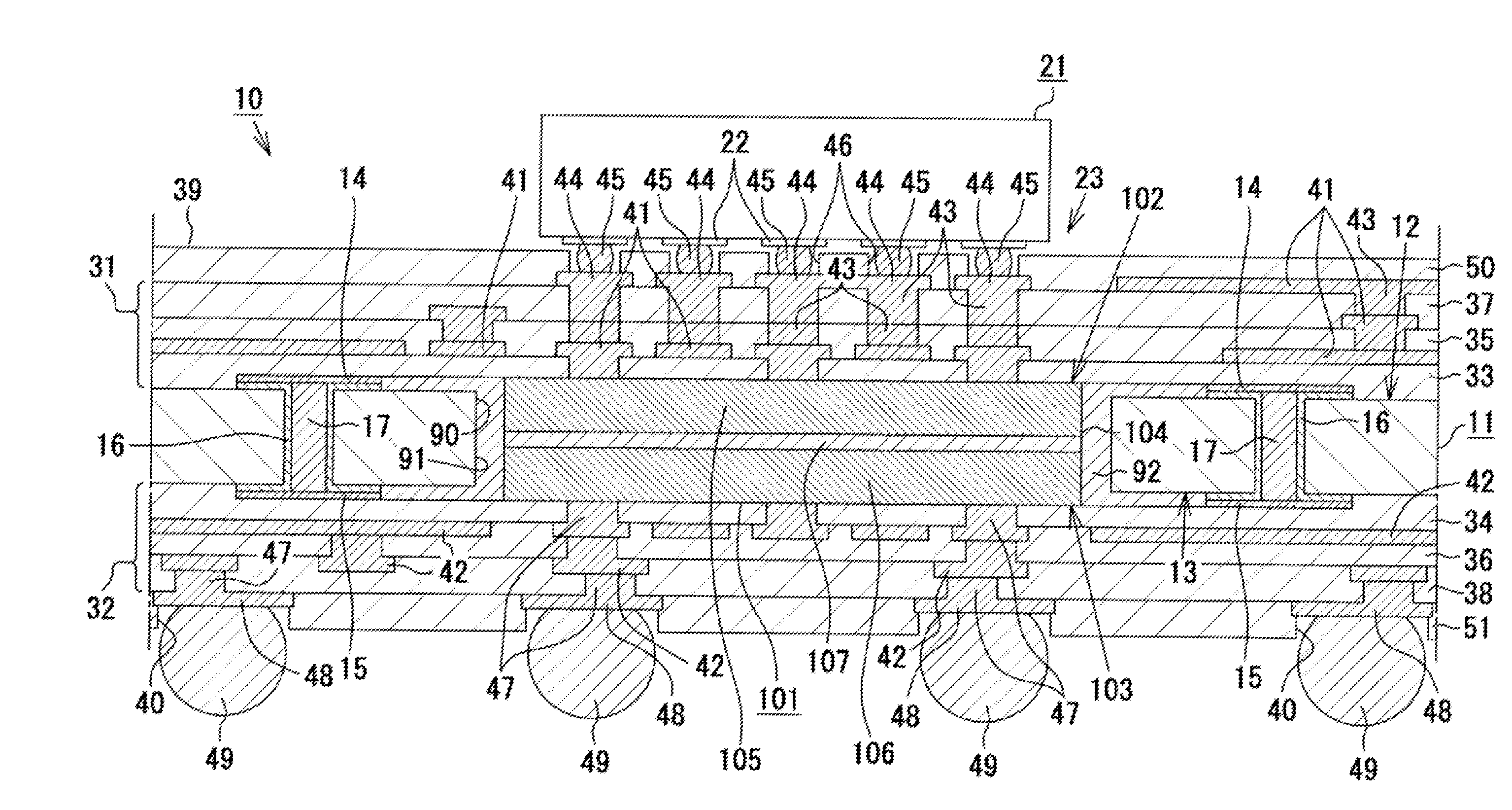
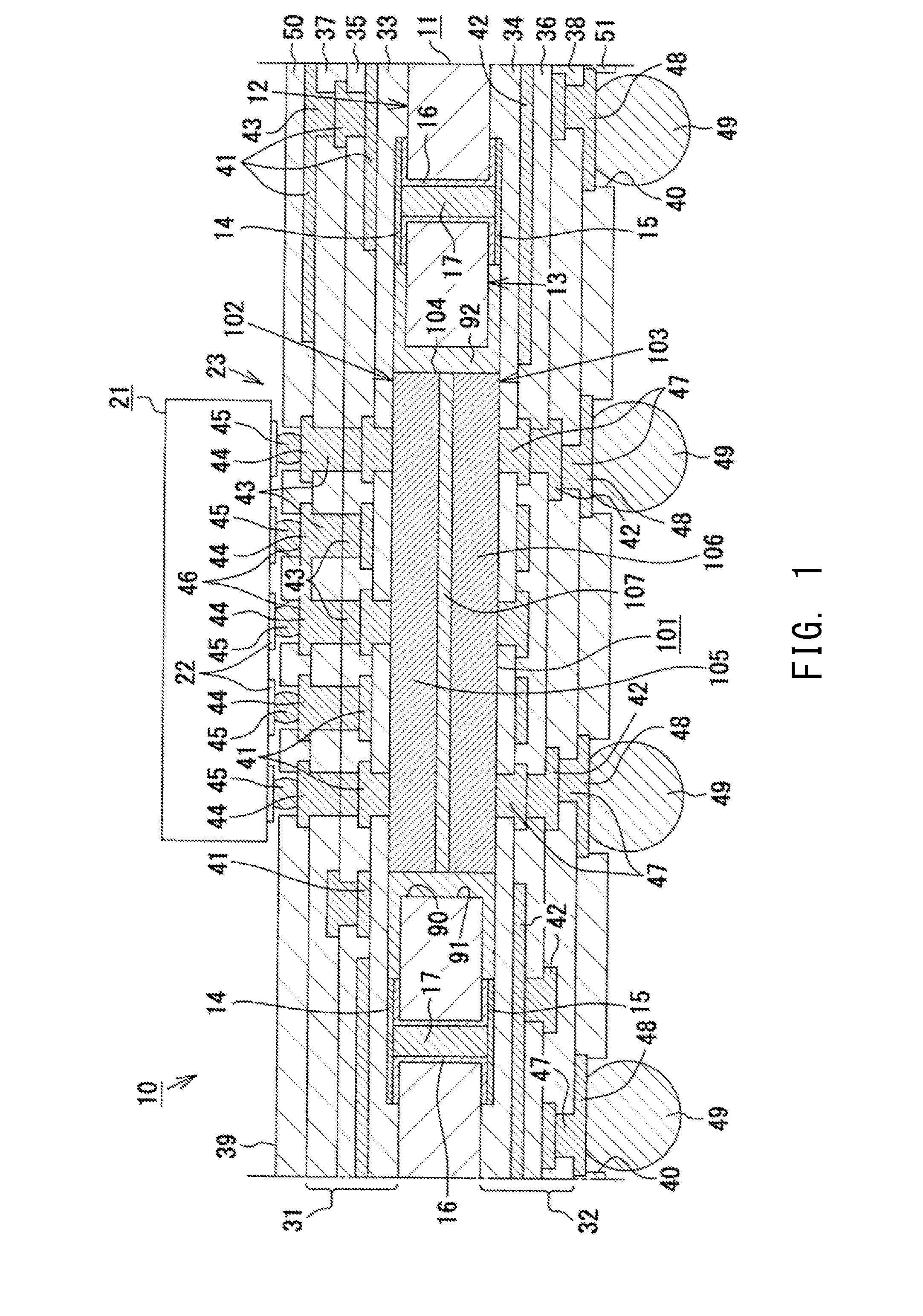
[0039]A multilayer wiring substrate according to an embodiment of the present invention will next be described in detail with reference to the drawings.

[0040]As shown in FIG. 1, a multilayer wiring substrate 10 of the present embodiment is a wiring substrate for mounting an IC chip thereon. The multilayer wiring substrate 10 includes a substantially square plate-like core substrate 11, a main-surface-side build-up layer 31 (a wiring laminate) formed on a core main-surface 12 (the upper surface in FIG. 1) of the core substrate 11, and a back-surface-side build-up layer 32 (a wiring laminate) formed on a core back-surface 13 (the lower surface in FIG. 1) of the core substrate 11.

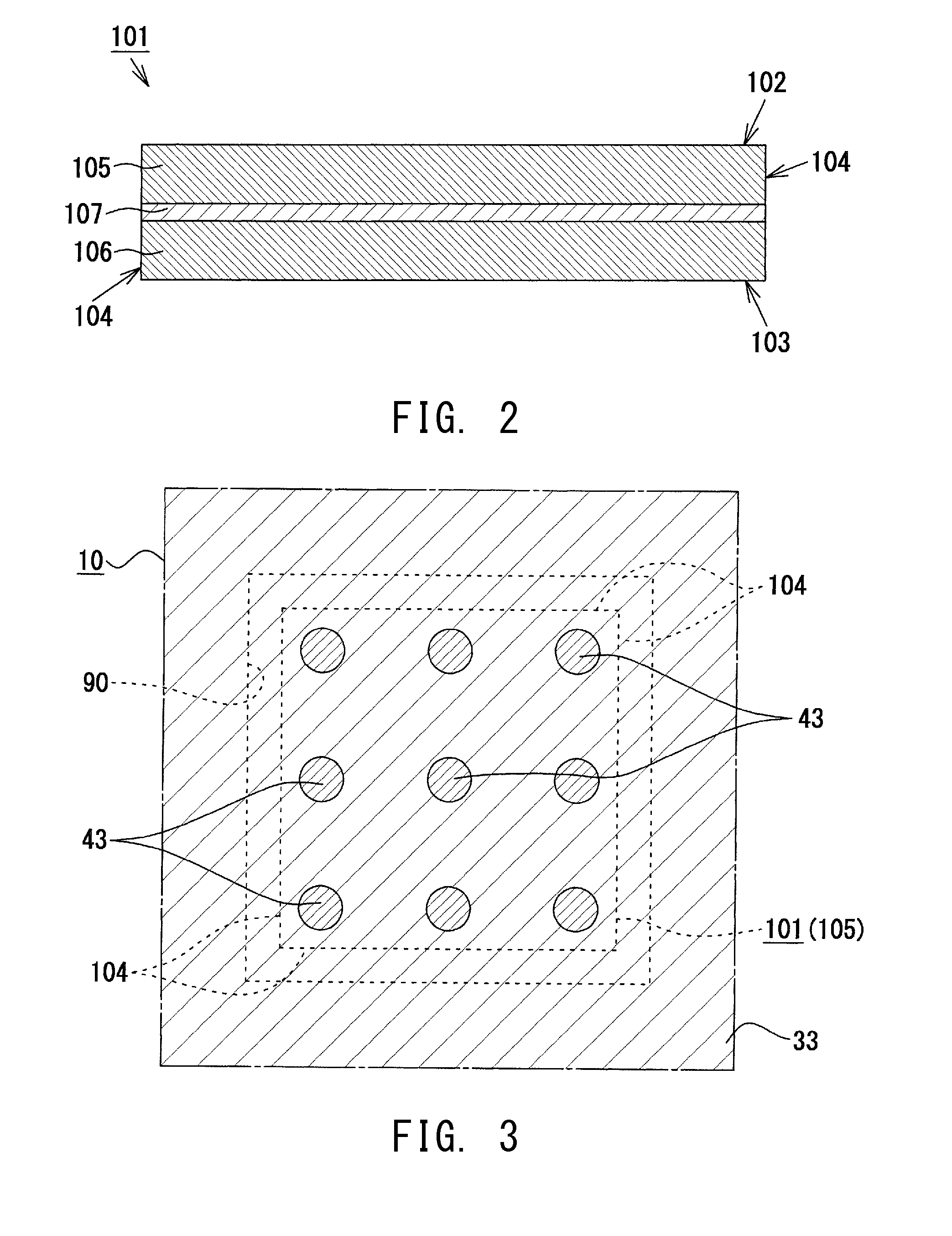
[0041]The core substrate 11 of the present embodiment has a square shape as viewed in plane, measuring 25 mm length×25 mm width. Also, the core substrate 11 has a thickness of 15 μm to 100 μm (46 μm in the present embodiment). The core substrate 11 is formed of a thermosetting resin (epoxy resin) and has a the...


PUM

PropertyMeasurementUnit
thicknessaaaaaaaaaa
thicknessaaaaaaaaaa
thicknessaaaaaaaaaa

Abstract

[Objective] To provide a multilayer wiring substrate in which, even when a core substrate is thinned, the core substrate can reliably accommodate a capacitor.
[Means for Solution] A multilayer wiring substrate 10 includes a sheetlike capacitor element 101, a resin filler 92, and via conductors 43 and 47. A sheetlike capacitor element 101 has an element main-surface 102 and an element back-surface 103, is configured such that a dielectric layer 107 is sandwiched directly between a main-surface-side electrode layer 105 exposed at the element main-surface 102 side and a back-surface-side electrode layer 106 exposed at the element back-surface 103 side, and is accommodated at least partially in an accommodation hole 90 such that a core main-surface 12 and the element main-surface 102 face the same direction. A resin filler 92 is charged into a gap between the sheetlike capacitor element 101 and an inner wall surface 91 of the accommodation hole 90. The via conductors 43 and 47 are provided in at least interlayer insulating layers 33 to 38 formed on the core main-surface 12 side, and are connected to at least the main-surface-side electrode layer 105.

Description

TECHNICAL FIELD[0001]The present invention relates to a multilayer wiring substrate which includes a core substrate and a wiring laminate formed on at least a core main-surface of the core substrate.BACKGROUND ART[0002]In association with recent increasing tendency toward higher operation speed and higher functionality of semiconductor integrated circuit devices (IC chips) used as, for example, microprocessors of computers, the number of terminals increases, and the pitch between the terminals tends to become narrower. Generally, a large number of terminals are disposed densely in an array on the bottom surface of an IC chip, and such a terminal group is flip-chip-connected to a terminal group on a motherboard. However, since a terminal group on the IC chip and a terminal group on the motherboard differ greatly in an inter-terminal pitch, difficulty is encountered in directly connecting the IC chip on the motherboard. Thus, usually, there is fabricated a package in which the IC chip...

Claims


Application Information

Patent Timeline
Patent Type & Authority Applications(United States)
IPC IPC(8): H05K1/02H05K1/11H01B1/02H01G4/12H01G4/008H05K1/18H01G4/30
CPCH05K1/0298H05K1/183H05K1/115H05K2201/10015H01G4/1227H01G4/008H01B1/026H01G4/30H05K3/4602H01G2/02H01G2/10H01G4/224H01L2224/16237H01L2924/15311H05K1/185H05K3/4697
Inventor YAMASHITA, DAISUKEKOBAYASHI, TERUYUKITORII, TAKUYAINOUE, MASAHIRO
Owner NGK SPARK PLUG CO LTD
Why Eureka
Try Eureka