Large area organic light emitting diode display

a light-emitting diode and organic technology, applied in the direction of thermoelectric device junction materials, electrical equipment, semiconductor devices, etc., can solve the problems of uneven brightness or luminance of display panels, cathode electrodes may not have even voltage distribution over the whole surface of display panels, and degradation of video quality, etc., to achieve the effect of lowering the lowering the surface resistance of cathode electrodes

Active Publication Date: 2015-05-28
LG DISPLAY CO LTD
View PDF4 Cites 59 Cited by
  • Summary
  • Abstract
  • Description
  • Claims
  • Application Information

AI Technical Summary

Benefits of technology

[0018]An object of the present invention is to provide a large area organic light emitting diode display having an auxiliary cathode electrode for lowering the surface resistance of the cathode electrode.
[0019]Another object of the present invention is to provide a large area organic light emitting diode display further including a protective electrode for preventing the auxiliary electrode for lowering the resistance of the cathode electrode being damaged in the manufacturing process conducted after forming the cathode electrode.

Problems solved by technology

When the cathode electrode CAT is made of a transparent conductive material for ensuring enough transmittivity, the surface resistance of the cathode electrode CAT is high so this may cause degradation of the video quality.
As a result, the cathode electrode CAT may not have even voltage distribution over the whole surface of the display panel.
This may cause the unevenness of the brightness or luminance of the display panel.
Especially, as the area of the organic light emitting diode display is getting larger, the unevenness of the luminance or lightness may be severely caused.

Method used


Image

  • Large area organic light emitting diode display
  • Large area organic light emitting diode display
  • Large area organic light emitting diode display

Examples


first embodiment

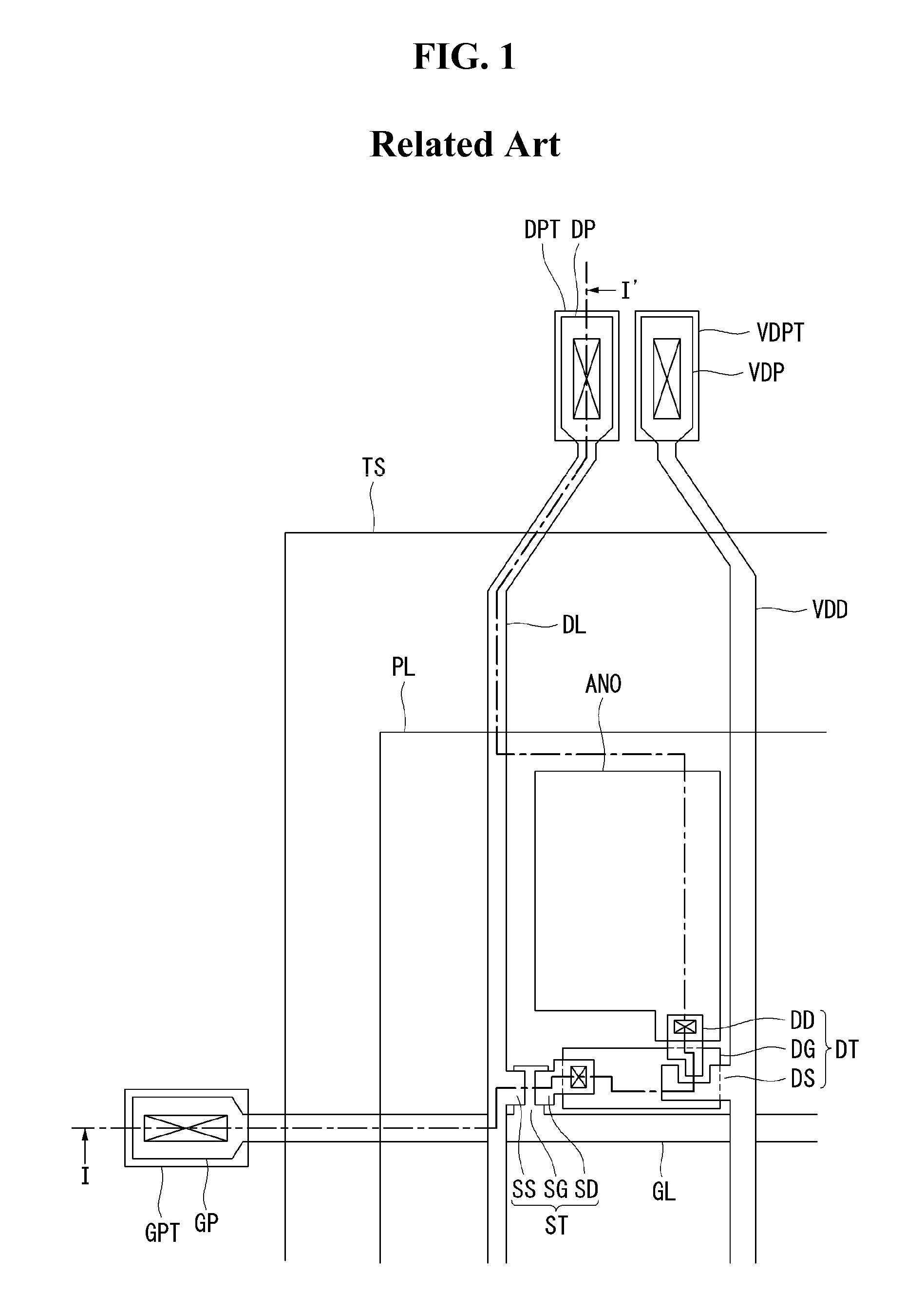
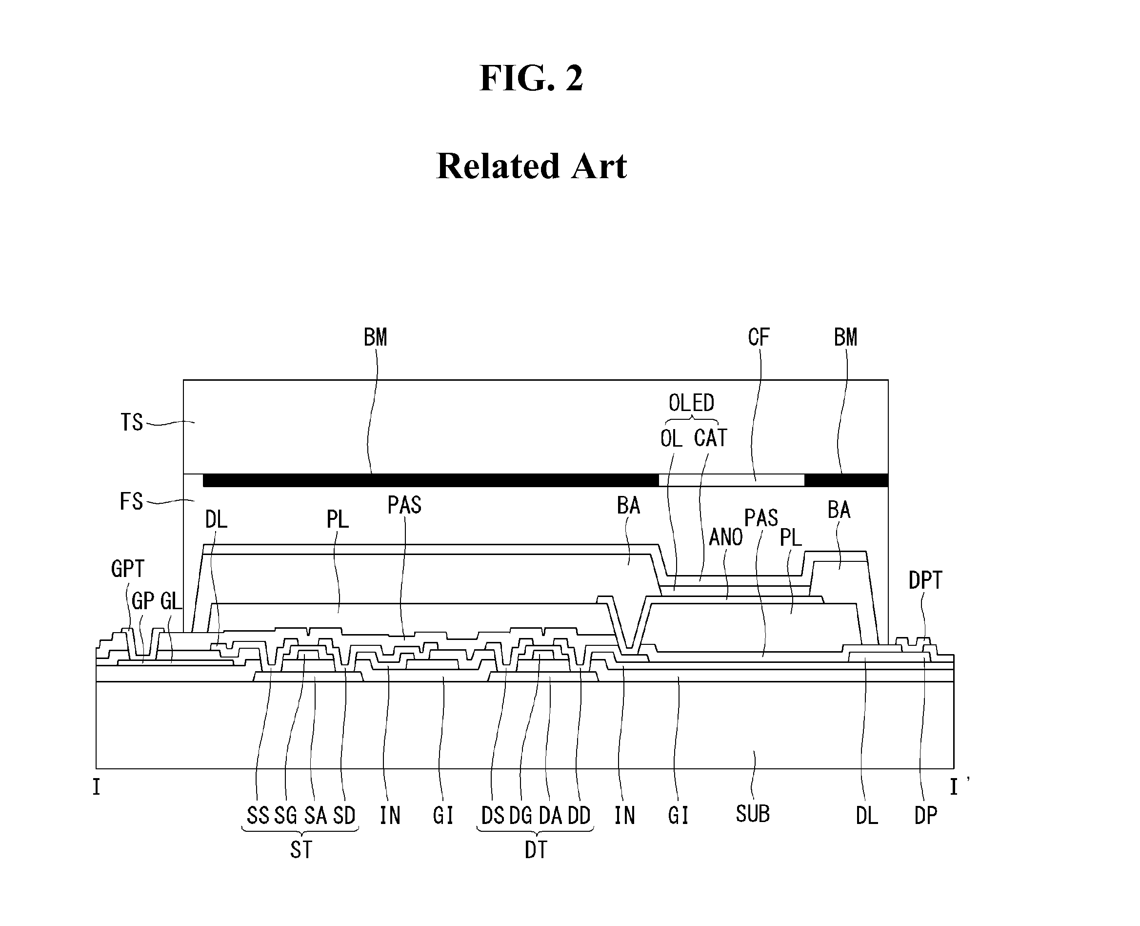
[0035]Referring to FIGS. 3 and 4, we will explain about the present disclosure. One of the main features of the present disclosure is at the structure of the auxiliary (or, assistance) cathode electrode for lowering the resistance of the cathode electrode. Therefore, we will not explain in detail about the thin film transistor and / or the organic light emitting diode having the similar structure of the related art.

[0036]At first, referring to FIG. 3, we will explain about the plane structure of the organic light emitting diode display according to the first embodiment in detail. An organic light emitting diode display according to the first embodiment of the present disclosure comprises a substrate SUB including a display area AA for representing the video information and a non-display area NA having various elements for driving the elements in the display area AA. In the display area AA, a plurality of pixel areas PA disposed in a matrix manner are defined. In FIG. 3, the pixel area...

second embodiment

[0065]Referring to FIGS. 5, 6A and 6B, an organic light emitting diode display according to the present disclosure comprises a substrate SUB including a non-display area NA and a display area AA. In the non-display area, a gate driving integrated circuit GIP and a ground line Vss are disposed. In the display area, a switching thin film transistor ST, a driving thin film transistor DT and an organic light emitting diode OLED are disposed.

[0066]The gate driving integrated circuit GIP may include thin film transistors formed when the switching thin film transistor ST and the driving thin film transistor DT in the display area AA. The switching thin film transistor ST in the pixel area PA has a gate electrode SG, a gate insulating layer GI, a channel layer SA, a source electrode SS and a drain electrode SD. In addition, the driving thin film transistor DT has a gate electrode DG connected to the drain electrode SD of the switching thin film transistor ST, the gate insulating layer GI, a...

third embodiment

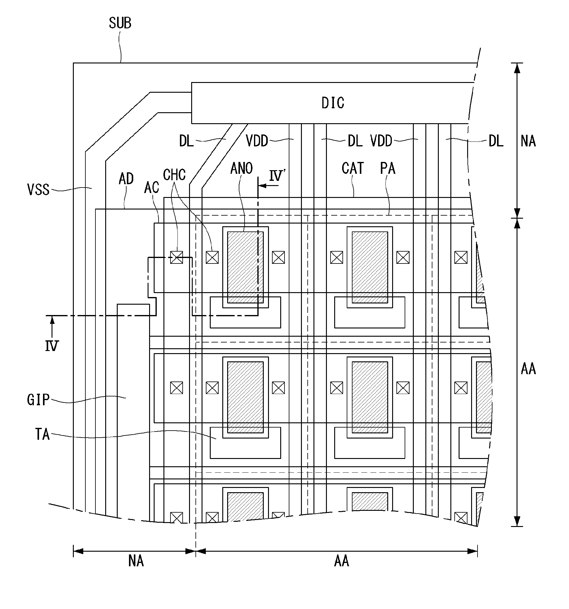
[0084]The organic light emitting diode display according to the present disclosure comprises a substrate SUB including a display area AA and a non-display area NA. The display area AA includes elements for representing the video information and the non-display area NA includes various elements for driving the elements in the display area AA. In the display area AA, a plurality of pixel areas PA are defined as arraying in a matrix manner.

[0085]In each pixel area PA, an organic light emitting diode OLED and thin film transistors ST and DT driving the organic light emitting diode OLED are disposed. The thin film transistors ST and DT are disposed within the thin film transistor area TA defined at one side of the pixel area PA. The organic light emitting diode OLED includes an anode electrode ANO, a cathode electrode CAT and an organic light emission layer OL inserted between these two electrodes. The actual emission area is decided by the overlapped area of the organic light emission l...


PUM


Abstract

A large area organic light emitting diode display is provided. The organic light emitting diode display comprises a substrate including a display area defining a plurality of pixel areas in a matrix manner and a non-display area surrounding the display area; a thin film transistor disposed in each pixel area; an auxiliary cathode electrode disposed at the same layer with an element of the thin film transistor; a planar layer on the thin film transistor and the auxiliary cathode electrode; an anode electrode connected to the thin film transistor and disposed in each pixel area on the planar layer; an organic light emission layer disposed on the anode electrode; a cathode electrode covering the whole surface of the display area on the organic light emission layer; and a protective electrode covering the auxiliary cathode electrode exposed through a cathode contact hole and contacting the cathode electrode.

Description

[0001]This application claims the benefit of Korea Patent Application No. 10-2013-0145839 filed on Nov. 28, 2013, which is incorporated herein by reference for all purposes as if fully set forth herein.BACKGROUND OF THE INVENTION[0002]1. Field of the Invention[0003]The present disclosure relates to a large area organic light emitting diode display, and more particularly, to an organic light emitting diode display having an auxiliary cathode electrode for lowering the surface resistance of the cathode electrode and a protective electrode for preventing the auxiliary cathode electrode.[0004]2. Discussion of the Related Art[0005]Nowadays, various flat panel display devices are developed for overcoming many drawbacks of the cathode ray tube such as heavy weight and bulk volume. The flat panel display devices include the liquid crystal display device (or LCD), the field emission display (or FED), the plasma display panel (or PDP) and the electroluminescence device (or EL).[0006]FIG. 1 is...

Claims


Application Information

Patent Timeline
Patent Type & Authority Applications(United States)
IPC IPC(8): H01L27/32H01L51/52
CPCH01L51/5228H01L27/3279H10K59/131H10K50/824H10K59/00H10K50/80H10K59/1315
Inventor MOON, JINYOUNGBOO, SAMYUL
Owner LG DISPLAY CO LTD
Why Eureka
Try Eureka