Method for fabricating nanoantenna array, nanoantenna array chip and structure for lithography

a nanoantenna array and array chip technology, applied in the field of nanoantenna array, nanoantenna array chip and structure for lithography, can solve the problems of inconvenient fabrication inability to fabricate large-area array chips, and inability to meet the requirements of large-area array chips, etc., to achieve the enhancement of local electric fields and improve sensitivity to the change of surrounding environments. , the effect of easy implementation

a nanoantenna array and array chip technology, applied in the field of nanoantenna array, nanoantenna array chip and structure for lithography, can solve the problems of inconvenient fabrication inability to fabricate large-area array chips, and inability to meet the requirements of large-area array chips, etc., to achieve the enhancement of local electric fields and improve sensitivity to the change of surrounding environments. , the effect of easy implementation

US20150146180A1Active Publication Date: 2015-05-28KOREA INST OF SCI & TECH

Image

  • Method for fabricating nanoantenna array, nanoantenna array chip and structure for lithography
  • Method for fabricating nanoantenna array, nanoantenna array chip and structure for lithography
  • Method for fabricating nanoantenna array, nanoantenna array chip and structure for lithography

Examples


Embodiment Construction

[0039]Hereinafter, embodiments of the present disclosure will be described in detail with reference to the accompanying drawings.

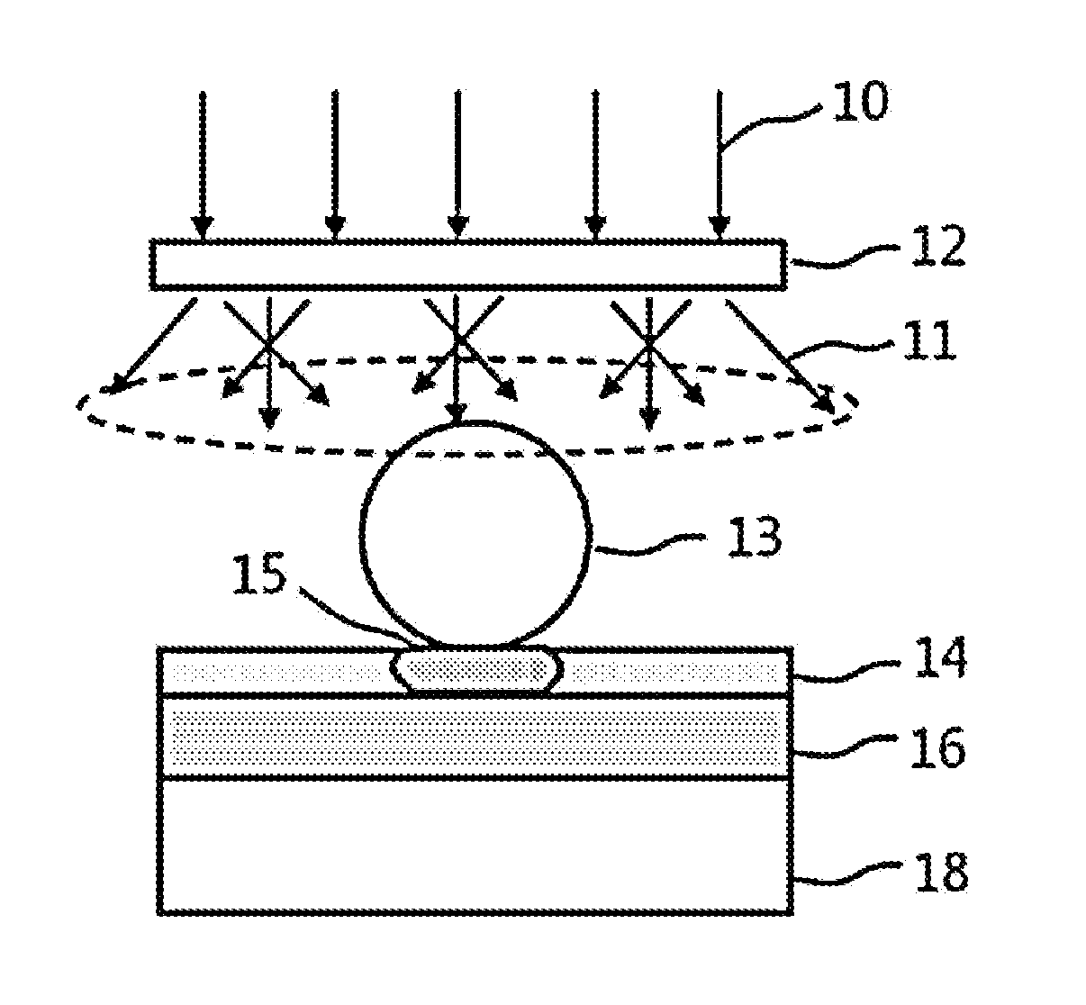
[0040]FIG. 1 is a schematic diagram showing an exemplary processing unit for performing a method for fabricating a nanoantenna array (hereinafter, also referred to as a nanoantenna array fabricating method) according to an embodiment of the present disclosure. The processing unit may be a structure for lithography according to an embodiment of the present disclosure, and the structure for lithography may include a linear diffuser 12, a focusing layer having an array of dielectric microstructures 13 and a resist layer 14.

[0041]Referring to FIG. 1, the nanoantenna array fabricating method according to an embodiment will be described. First, the resist layer 14 is formed on a substrate 18. The resist layer 14 may be configured to have a dual-layered structure having an additional lower undercut-forming layer 16, which is etched by most developing solutions, a...


PUM

PropertyMeasurementUnit
resonance wavelengthaaaaaaaaaa
diameteraaaaaaaaaa
resonance wavelengthaaaaaaaaaa

Abstract

A method for fabricating a nanoantenna array may include forming a resist layer on a substrate, forming a focusing layer having a dielectric microstructure array on the resist layer, diffusing light one-dimensionally in a specific direction by using a linear diffuser, forming an anisotropic pattern on the resist layer by illuminating the light diffused by the linear diffuser on the focusing layer and the resist layer, depositing a material suitable for a plasmonic resonance onto the substrate and the resist layer on which the pattern is formed, and forming a nanoantenna array on the substrate by removing the resist layer and the material deposited on the resist layer. A light diffusing angle by the linear diffuser and a size of the dielectric microstructure are determined based on an aspect ratio of the pattern to be formed.

Description

CROSS-REFERENCE TO RELATED APPLICATION[0001]This application claims priority to Korean Patent Application No. 10-2013-0143068, filed on Nov. 22, 2013, and all the benefits accruing therefrom under 35 U.S.C. ยง119, the contents of which in its entirety are herein incorporated by reference.BACKGROUND[0002]1. Field[0003]Embodiments relate to a process for forming a nanoantenna array, a nanoantenna array chip and a structure for lithography, which is used for forming a nanoantenna array.[0004]2. Description of the Related Art[0005]A metallic nanostructure shows a localized surface plasmon resonance phenomenon in a specific wavelength region due to a dielectric confinement effect of free electrons. At a resonance wavelength, a local electric field near a metallic nanostructure is strongly enhanced, and a characteristic optical absorption or scattering behavior occurs in proportion to the intensity of the local electric field.[0006]Since the characteristics of localized surface plasmon res...

Claims


Application Information

Patent Timeline
28 May 2015
Publication
US20150146180A1
IPC
G02B5/00; G01N21/552; G02B5/02; G03F7/38
CPC
G02B5/008; G02B5/02; G01N21/554; G03F7/38; G02B5/0278; G03F7/2014; G03F7/70375; G02B5/00
Inventors
LEE, KYEONG SEOK; KIM, WON MOK