
Correction device and correction method for light reception power monitor

Active Publication Date: 2015-06-18
NEC CORP
View PDF3 Cites 6 Cited by
  • Summary
  • Abstract
  • Description
  • Claims
  • Application Information

AI Technical Summary

Benefits of technology

The correction device and method described in this patent text have several technical effects. First, by reducing the number of reference values and storing them in a correction table, the storage capacity of the table is reduced. Second, by using nonlinear calculation formulas for each range of reference values, a correction value can be calculated even for an input value that does not match any of the reference values in the table. Third, the correction values are finely set in a high-order curve interpolation, which causes a smaller change rate in the reference values than a linear interpolation, resulting in higher precision of the correction value for an input value.

Problems solved by technology

However, the use of such an MPU makes it difficult to calculate an actual value on the basis of a measured value of a light reception power monitor by executing high load processing such as a fourth-order interpolation in a short time.

Method used


Image

  • Correction device and correction method for light reception power monitor
  • Correction device and correction method for light reception power monitor
  • Correction device and correction method for light reception power monitor

Examples


first embodiment

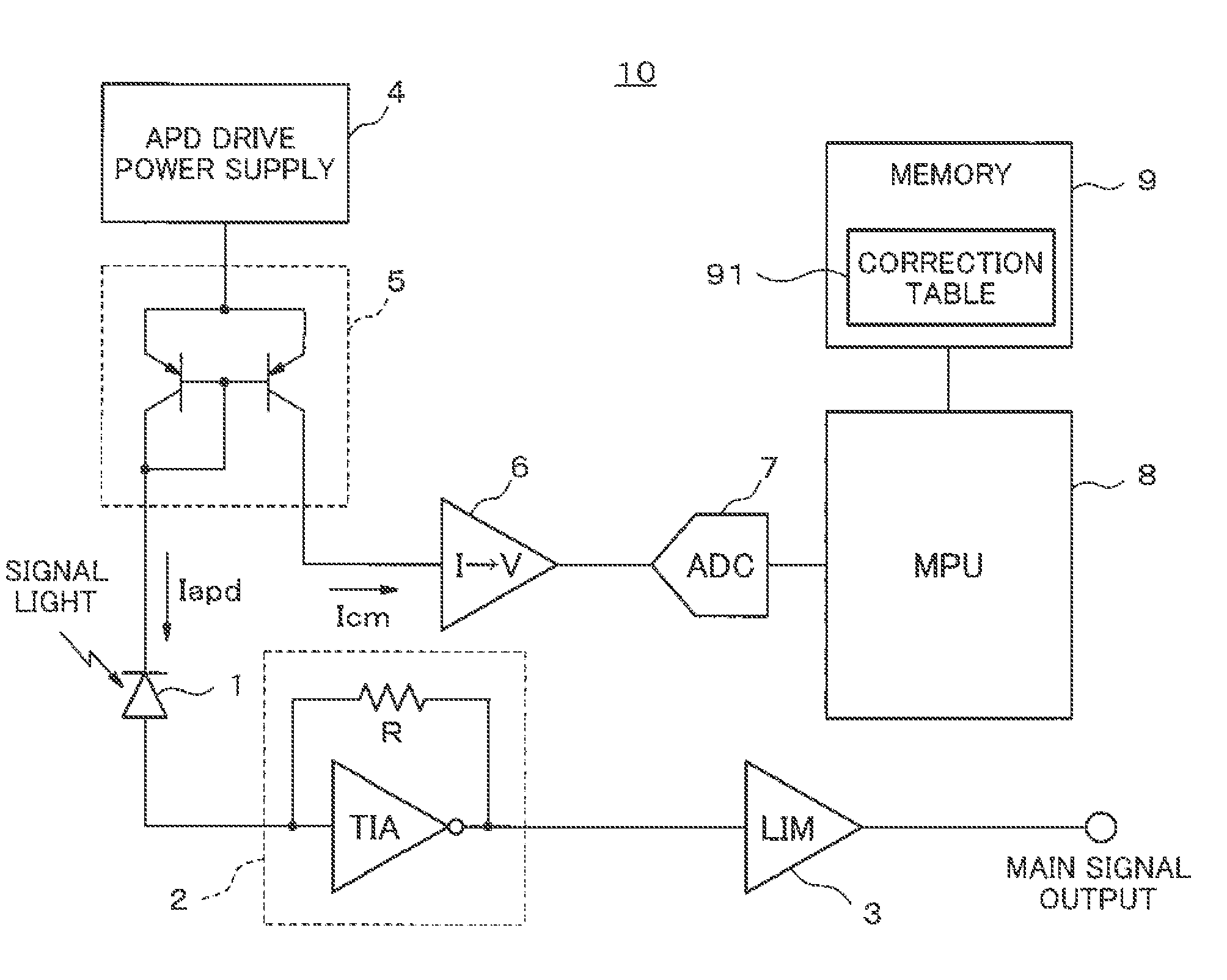
[0037]FIG. 1 is a block diagram of an optical module 10 according to a first embodiment of the present invention. The optical module 10 includes an APD (Avalanche Photodiode) 1, a TIA (Transimpedance Amplifier) 2, a LIM (Limiting Amplifier) 3, an ADP drive power supply 4, a current mirror circuit 5, a current voltage conversion circuit 6, an A / D converter 7, an MPU 8, and a memory 9. The memory 9 has a correction table 91. The optical module 10 is provided with a light reception function for converting signal light received by the APD 1 into a main signal output and a light reception power monitor function for measuring light reception power of the APD 1.

[0038]The APD 1 as a light receiving element outputs a current Iapd corresponding to received signal light. The TIA 2 as a pre-amplifier amplifies the current Iapd generated by the APD 1 with a gain proportional to a resistance value of a feedback resistor R to convert into a voltage signal. The LIM 3 as a post-amplifier amplifies t...

second embodiment

[0065]Next, a detailed description will be given of a second embodiment of the present invention. FIG. 7 is a block diagram of an optical module 10a according to the second embodiment of the invention. A basic structure of the optical module 10a according to the second embodiment is the same as that of the optical module 10 according to the first embodiment. Thus, the same reference numerals are given to constituent elements of the module 10a and a description thereof will be omitted.

[0066]Unlike the optical module 10, the memory 9 of the optical module 10a stores two kinds of tables, i.e. a correction table 91a and a calculation information table 92a.

[0067]FIG. 8 is a table depicting a storage content of the correction table 91a. The correction table 91a of FIG. 8 is created in connection with a case in which the A / D converter 7 has a resolution of 12 bits and converts an input voltage into an ADC measured value ad in a range of from “0” to “4095”. The correction table 91a is a ta...

third embodiment

[0089]Next, a description will be given of an optical module 10b (not shown) according to a third embodiment of the present invention. A basic structure of the optical module 10b of the third embodiment is the same as that of the optical module 10a of the second embodiment and thus a detailed description thereof will be omitted. Unlike the optical module 10a (see FIG. 7), the optical module 10b stores the correction table 91a and the calculation information table 92b in the memory 9.

[0090]FIG. 12 depicts a storage content of the correction table 91b stored in the memory 9 of the optical module 10b according to the third embodiment. Like the correction table 91a according to the second embodiment (see FIG. 8), the correction table 91b according to the third embodiment is created in connection with the A / D converter 7 having a resolution of 12 bits. In the correction table 91b, in order to precisely correct light reception power when an input is small, the intervals between 64 ADC mea...


PUM


Abstract

The objective of the present invention is to quickly and precisely correct the measured value for light reception power to the actual value with few resources, by installing a correction device for a light reception power monitor for signal light in an optical module. The correction device is equipped with a correction table which is referenced when correcting the measured value for the light reception power of signal light, and in this correction table multiple correction values are stored in advance on the basis of the correspondence relationships between multiple reference values and multiple actual values. In the correction table, for segments wherein the change in the actual values with respect to the change in the measured values is small, the interval between the reference values is made smaller and more correction values are stored than for segments wherein the change in the actual values with respect to the change in the measured values is large. When an input value indicating the measured value for the light reception power of the signal light matches a reference value in the correction table, the correction device reads from the correction table the correction value corresponding to the reference value. When an input value does not match a reference value in the correction table, the correction device calculates a correction value in accordance with a prescribed calculation formula on the basis of the input value.

Description

TECHNICAL FIELD[0001]The present invention relates to a device and a method for correcting a measured value of a light reception power monitor in an optical module having a light reception function using an APD (Avalanche Photodiode).[0002]This application is based upon and claims the benefit of priority from Japanese Patent Application No. 2012-180414, filed on Aug. 16, 2012, the content of which is incorporated herein by reference.BACKGROUND ART[0003]Conventionally, a technique relating to a light reception power monitor of an optical module has been developed and disclosed in various pieces of literature. Patent Literature 1 discloses a light power meter for correcting light reception sensitivity using a correction coefficient in order to precisely measure light power of measured light even when light reception sensitivity of a light receiving element deteriorates over time. Patent literature 2 discloses an optical LAN system adapted to control a light output signal of an optical...

Claims


Application Information

Patent Timeline
IPC IPC(8): G01J1/18
CPCG01J2001/186G01J1/18H04B10/69H03M1/1038G01J2001/444G01J2001/4466G01J1/44
Inventor NOMURA, RINTARO
Owner NEC CORP
Features
  • Generate Ideas
  • Intellectual Property
  • Life Sciences
  • Materials
  • Tech Scout
  • Unparalleled Data Quality
  • Higher Quality Content
  • 60% Fewer Hallucinations
Learn More