

Sulfur-containing thin films
a technology of sulfur-containing thin films and metal sulfide films, which is applied in the direction of coatings, metallic material coating processes, chemical vapor deposition coatings, etc., can solve the problems of severe deterioration of the function of electronic devices, problems with these new channel materials,
- Summary
- Abstract
- Description
- Claims
- Application Information
AI Technical Summary
Benefits of technology
Problems solved by technology
Method used
Image

Examples
example 1
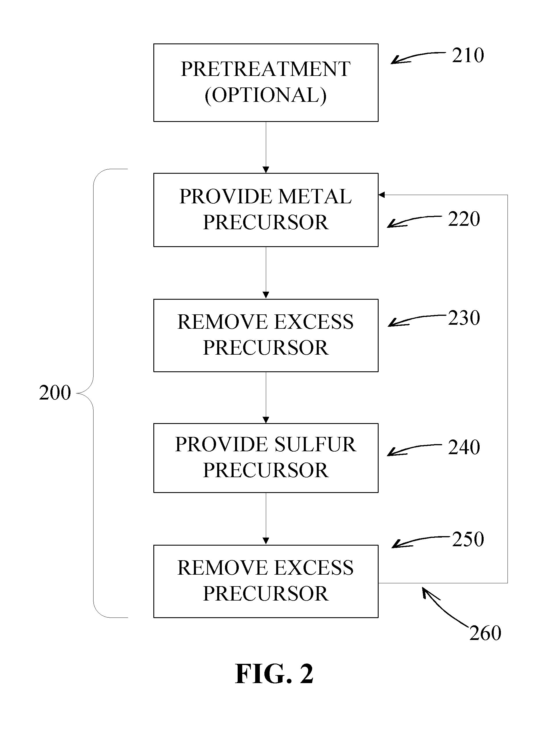
[0198]A number of metal sulfide films were formed using an ALD process in which process conditions were varied. The metal chosen for the metal sulfide was magnesium and precursor was Mg(Cp)2, and the sulfur precursor was (NH4)2S extracted from a bubbler containing (NH4)2S solution in water. The metal and sulfide reactants or precursors were pulsed through a reaction space in an ALD process with pulse times ranging from 40 ms to 50 ms. Growth rates varied between about 0.2 Å / cycle and about 0.5 Å / cycle were observed with the faster growth rates occurring initially and the growth rate slowing to a steady 0.2 Å / cycle. The reaction temperature was varied from about 250° C. to about 300° C.
[0199]The resulting films were analyzed using XRR analysis, which determined a MgS density of about 2.6 g / cm3. This is within the range of bulk MgS density (2.6-2.8 g / cm3). It was also determined by XRD analysis that a pulsing time for the sulfur precursor of about 50 ms achieved an MgS-dominated film ...
example 2
[0201]A number of metal sulfide films were formed using an ALD process in which process conditions were varied. Prior to film formation, the substrates were subjected to a pretreatment process comprising exposure to HCl and H2S. The metal chosen for the metal sulfide was magnesium, and the precursor was Mg(Cp)2, and the sulfur precursor was H2S. The metal and sulfide reactants or precursors were pulsed through a reaction space in an ALD process with pulse times ranging from about 50 ms to about 3 s. Growth rates varied between about 0.2 Å / cycle and about 0.5 Å / cycle with the faster growth rates occurring initially and the growth rate slowing to a steady 0.2 Å / cycle. The reaction temperature was about 250° C. After deposition was complete, the films were subjected to a post deposition treatment comprising exposure to gas mixture of N2 and H2 at 400° C. The resulting films were analyzed using XRR analysis, which determined a MgS density of about 2.6 g / cm3. This is within the range of ...
example 3
[0203]In this example, a comparison was made between two metal oxide semiconductor capacitors (MOSCAPs) formed on respective InGaAs substrates. A first MOSCAP was formed with an Al2O3 interface layer, and a second MOSCAP was formed with an MgS interface layer formed according to the present disclosure in which Mg(Cp)2 served as the metal precursor, and H2S served as the sulfur precursor. The respective features and results obtained are contained in Table 1 below.
TABLE 1Comparison of physical properties usingMgS vs. Al2O3 interfacial layers.MetricBenchmark LayerMgS Interface LayerStructurePt gated MOSCAP onPt gated MOSCAP onIn0.53Ga0.47AsIn0.53Ga0.47AsEx-situHCl wet cleanHCl wet cleanpretreatmentIn-situH2SH2SpretreatmentInterface—MgS deposited with 11Layercycles to achieve a thicknessbetween ~10 Å and ~15 ÅHigh-k Layer10 Å Al2O3 and10 Å Al2O3 and30 Å of HfO230 Å of HfO2Post high-kH2 / N2 annealingH2 / N2 annealingtreatmentat 400° C.at 400° C.CET1.6 nm2.3 nmDit at midgap~1.4E12(eV−1cm−2)D...
PUM
| Property | Measurement | Unit |
|---|---|---|
| Time | aaaaa | aaaaa |
| Time | aaaaa | aaaaa |
| Thickness | aaaaa | aaaaa |
Abstract
Description
Claims
Application Information