Semiconductor device, method of manufacturing semiconductor device, solid-state image pickup unit, and electronic apparatus

a semiconductor and semiconductor technology, applied in thermoelectric devices, basic electric elements, final product manufacture, etc., can solve problems such as increasing dark current, and achieve the effect of improving sensitivity, reducing light transmittance of electrodes, and easy current drawing

Active Publication Date: 2015-07-02
SONY SEMICON SOLUTIONS CORP
View PDF1 Cites 29 Cited by
  • Summary
  • Abstract
  • Description
  • Claims
  • Application Information

AI Technical Summary

Benefits of technology

[0005]However, transmittance of the metal film is extremely low; therefore, even if the metal film is extremely thin, light transmittance of the electrode may be reduced by inserting the metal film.
[0008]In the semiconductor device of the embodiment of the present disclosure, the first electrode and the second electrode are configured of the same transparent conductive material, and the oxygen amount at the interface on the functional layer side of the first electrode is smaller than the oxygen amount at the interface on the functional layer side of the second electrode; therefore, a work function at the interface on the functional layer side of the first electrode is reduced.
[0030]According to the semiconductor device of the embodiment of the present disclosure, the first electrode and the second electrode are made of the same transparent conductive material, and the oxygen amount at the interface on the functional layer side of the first electrode is smaller than the oxygen amount at the interface on the functional layer side of the second electrode. Therefore, the work function is allowed to be adjusted without reducing light transmittance of electrodes. According to the solid-state image pickup unit of the embodiment of the present disclosure, the organic photoelectric conversion section is configured of the above-described semiconductor device of the embodiment of the present disclosure; therefore, a current is easily drawn, and sensitivity is improved. Moreover, according to the electronic apparatus of the embodiment of the present disclosure, the above-described solid-state image pickup unit of the embodiment of the present disclosure is included; therefore, image pickup with high image quality is allowed to be performed.
[0031]According to the first method of manufacturing the semiconductor device of the embodiment of the present disclosure, the inorganic oxide layer with a higher metal content ratio than that in the ideal composition is formed, and while the reduced layer is formed in a part or a whole in the thickness direction from the interface on the functional layer side of the first electrode by annealing treatment, the oxygen amount of the reduced layer is allowed to be smaller than the oxygen amount of the transparent conductive material. According to the second method of manufacturing the semiconductor device of the embodiment of the present disclosure, the first layer made of the inorganic oxide with a higher metal content ratio than that in the ideal composition or the metal and the second layer made of the inorganic oxide with a larger oxygen amount than the first layer are formed in this order on the first electrode, and while the reduced layer is formed in a part or a whole in the thickness direction from the interface on the functional layer side of the first electrode by annealing treatment, the oxygen amount of the reduced layer is allowed to be smaller than the oxygen amount of the transparent conductive material. According to the third method of manufacturing the semiconductor device of the embodiment of the present disclosure, the oxygen amount at the interface on the functional layer side of the second electrode is allowed to be larger than the oxygen amount at the interface on the functional layer side of the first electrode by annealing treatment. Therefore, the above-described semiconductor device of the embodiment of the present disclosure is allowed to be manufactured easily.

Problems solved by technology

Since transparent conductive materials typified by ITO have a large work function as described in, for example, PTL 1, hole injection into an organic film is likely to occur, thereby causing an increase in a dark current.

Method used


Image

  • Semiconductor device, method of manufacturing semiconductor device, solid-state image pickup unit, and electronic apparatus
  • Semiconductor device, method of manufacturing semiconductor device, solid-state image pickup unit, and electronic apparatus
  • Semiconductor device, method of manufacturing semiconductor device, solid-state image pickup unit, and electronic apparatus

Examples


first embodiment

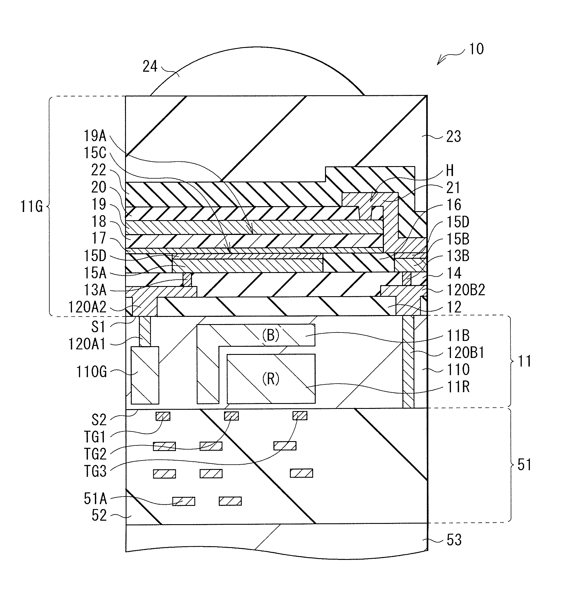
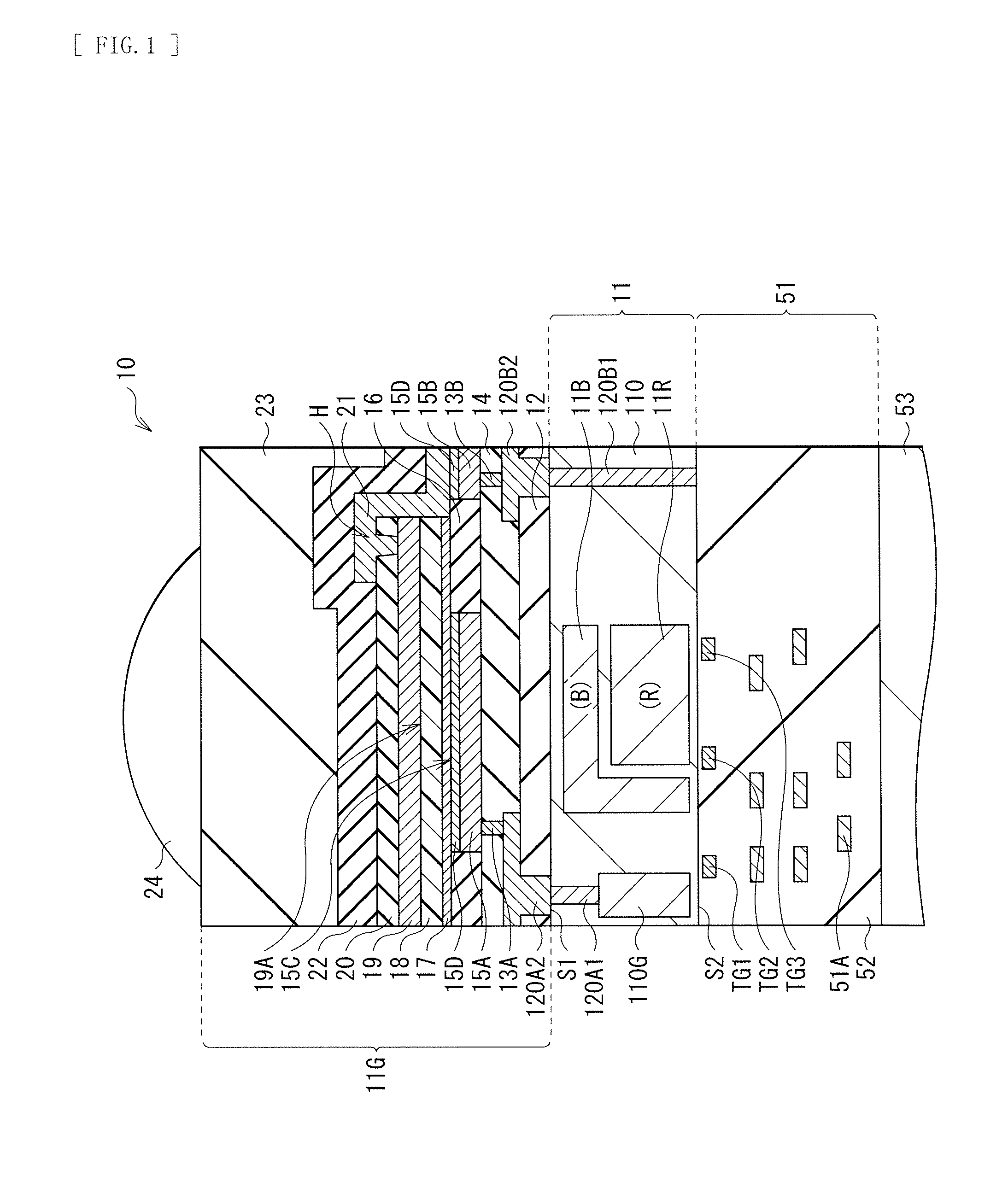
[0095]FIG. 1 illustrates a sectional configuration of a semiconductor device (a photoelectric conversion device) according to a first embodiment of the present disclosure. The photoelectric conversion device 10 may configure, for example, one pixel in a solid-state image pickup unit (that will be described later) such as a CCD (Charge Coupled Device) image sensor or a CMOS (Complementary Metal Oxide Semiconductor) image sensor.

[0096]The photoelectric conversion device 10 may have, for example, a configuration in which an organic photoelectric conversion section and an inorganic photoelectric conversion section that are configured to selectively detect light in wavelength ranges different from each other to perform photoelectric conversion are laminated in a vertical direction. Therefore, in the solid-state image pickup unit that will be described later, one pixel is capable of obtaining a plurality of kinds of color signals without using a color filter. More specifically, the photoe...

modification example 1

[0175]It is to be noted that in the above-described embodiment, a configuration in which the insulating film 16 is planarized and a difference in level between the insulating film 16 and the lower electrode 15 is reduced is exemplified; however, an insulating film 16A as illustrated in FIG. 28 may be used. In a photoelectric conversion device 10A of this modification example, the insulating film 16A includes openings H2 on the lower electrode 15A and on the wiring layer 15B to have a difference in level between the lower electrode 15A and the wiring layer 15B. However, side surfaces of the openings H2 have a slightly tapered shape, and the inorganic oxide layer 17 and the organic photoelectric conversion layer 18 are continuously provided on a top surface and a side surface of the insulating film 16A and in the opening H2 without being separated by the difference in level. The reduced layer 15D is provided to a region where the lower electrode 15A or the wiring layer 15B and the ino...

second embodiment

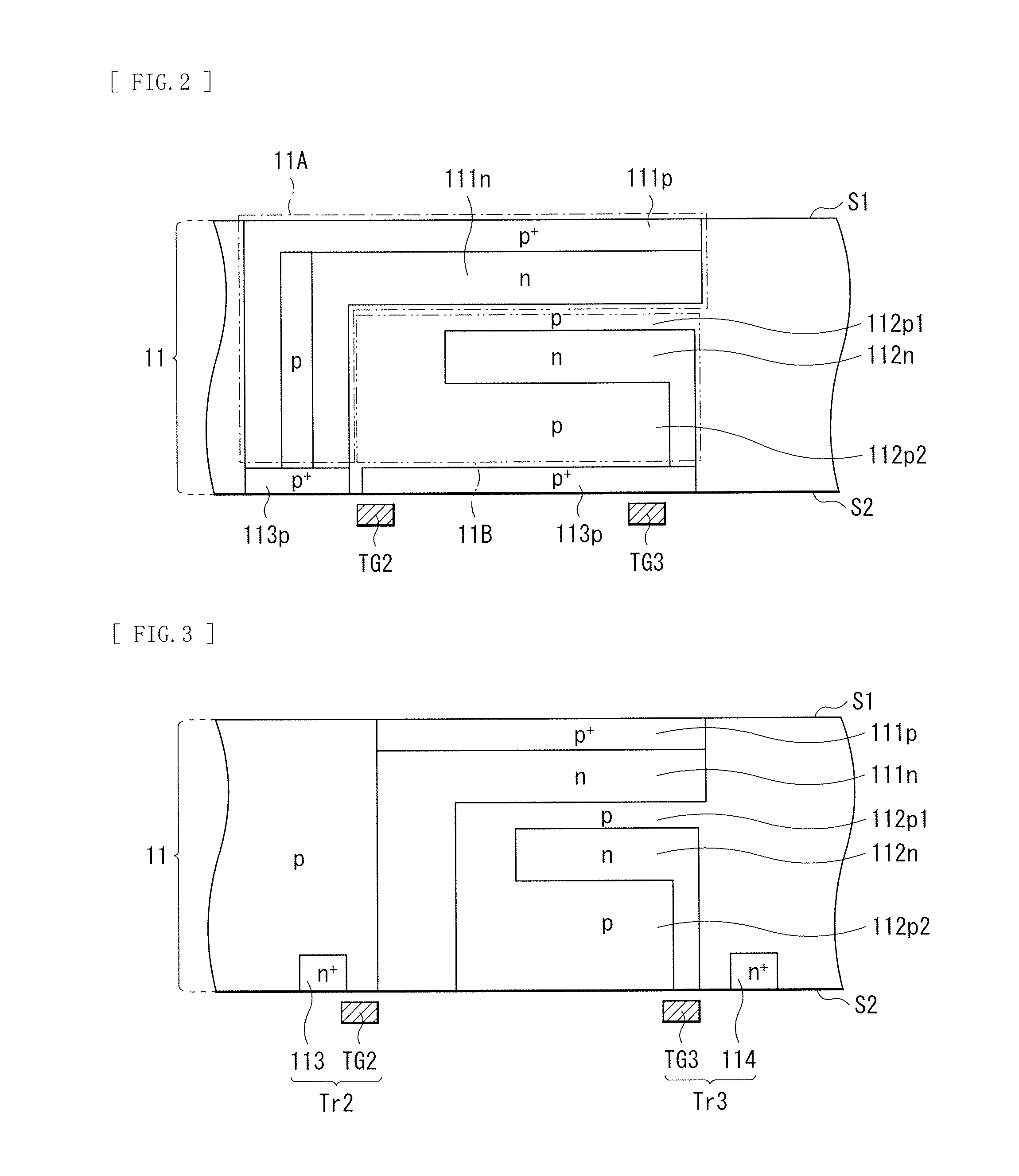
[0179]FIG. 33 illustrates a sectional configuration of a semiconductor device (a photoelectric conversion device) according to a second embodiment of the present disclosure. The photoelectric conversion device 10B includes a first inorganic oxide layer 17A and a second inorganic oxide layer 17B between the reduced layer 15D and the organic photoelectric conversion layer 18. Except for this, the photoelectric conversion device 10B of this embodiment has a configuration, functions, and effects similar to those in the above-described first embodiment. Therefore, description will be given with like reference numerals indicating like components corresponding to the first embodiment.

[0180]The inorganic oxide layer 17 in the above-described first embodiment has both a function as a hole block layer and a function as a work function adjustment layer that accelerates reduction of the lower electrode 15A in a manufacturing process to adjust the work function at the interface 15C of the lower ...


PUM


Abstract

There are provided a semiconductor device capable of adjusting a work function without reducing light transmittance of an electrode, a method of manufacturing this semiconductor device, a solid-state image pickup unit including this semiconductor device, and an electronic apparatus including this solid-state image pickup action. The semiconductor device includes a functional layer between a first electrode and a second electrode, the functional layer including an organic film, in which the first electrode and the second electrode are made of a same transparent conductive material, and an oxygen amount at an interface on the functional layer side of the first electrode is smaller than an oxygen amount at an interface on the functional layer side of the second electrode.

Description

TECHNICAL FIELD[0001]The present disclosure relates to a semiconductor device including an organic film, a method of manufacturing the semiconductor device, a solid-state image pickup unit including the semiconductor device, and an electronic apparatus including the solid-state image pickup unit.BACKGROUND ART[0002]Semiconductor devices such as organic photoelectric conversion devices, organic EL (Electroluminescence) devices, and organic solar cell devices may have, for example, a configuration in which an organic film is sandwiched between a lower electrode (a first electrode) and an upper electrode (a second electrode). Such semiconductor devices may need light transmittance depending on the purpose of use, and for such a purpose, a transparent conductive film, for example, ITO (Indium Tin Oxide) is used as the upper electrode and the lower electrode.[0003]Since transparent conductive materials typified by ITO have a large work function as described in, for example, PTL 1, hole i...

Claims


Application Information

Patent Timeline
Patent Type & Authority Applications(United States)
IPC IPC(8): H01L51/44H01L27/30H01L51/00
CPCH01L51/445H01L27/307H01L51/0021H01L27/1462H01L27/1464H01L27/14647H01L27/14685Y02E10/549Y02P70/50H10K39/32H10K30/82H10K2102/102H10K30/83H10K71/60
Inventor TAKIMOTO, KAORI
Owner SONY SEMICON SOLUTIONS CORP
Why Eureka
Try Eureka