Sputtering Target

Inactive Publication Date: 2015-07-16
JX NIPPON MINING& METALS CORP
View PDF11 Cites 4 Cited by
  • Summary
  • Abstract
  • Description
  • Claims
  • Application Information

AI Technical Summary

Benefits of technology

The invention helps prevent warping, detachment of the target from the backup plate, and cracks in large sputtering targets. It also enables more uniform deposition, reduces defects, and increases manufacturing efficiency.

Problems solved by technology

In manufacture of a semiconductor device, the costs for manufacturing an LSI Logic and a memory rapidly increase as a wiring width is becoming finer.
In particular, since high energy is loaded to a target during sputtering, a sputtering surface of the target becomes very hot at several hundreds degrees Celsius, and disadvantageously the target itself will be deformed.

Method used


Image

  • Sputtering Target
  • Sputtering Target
  • Sputtering Target

Examples


examples

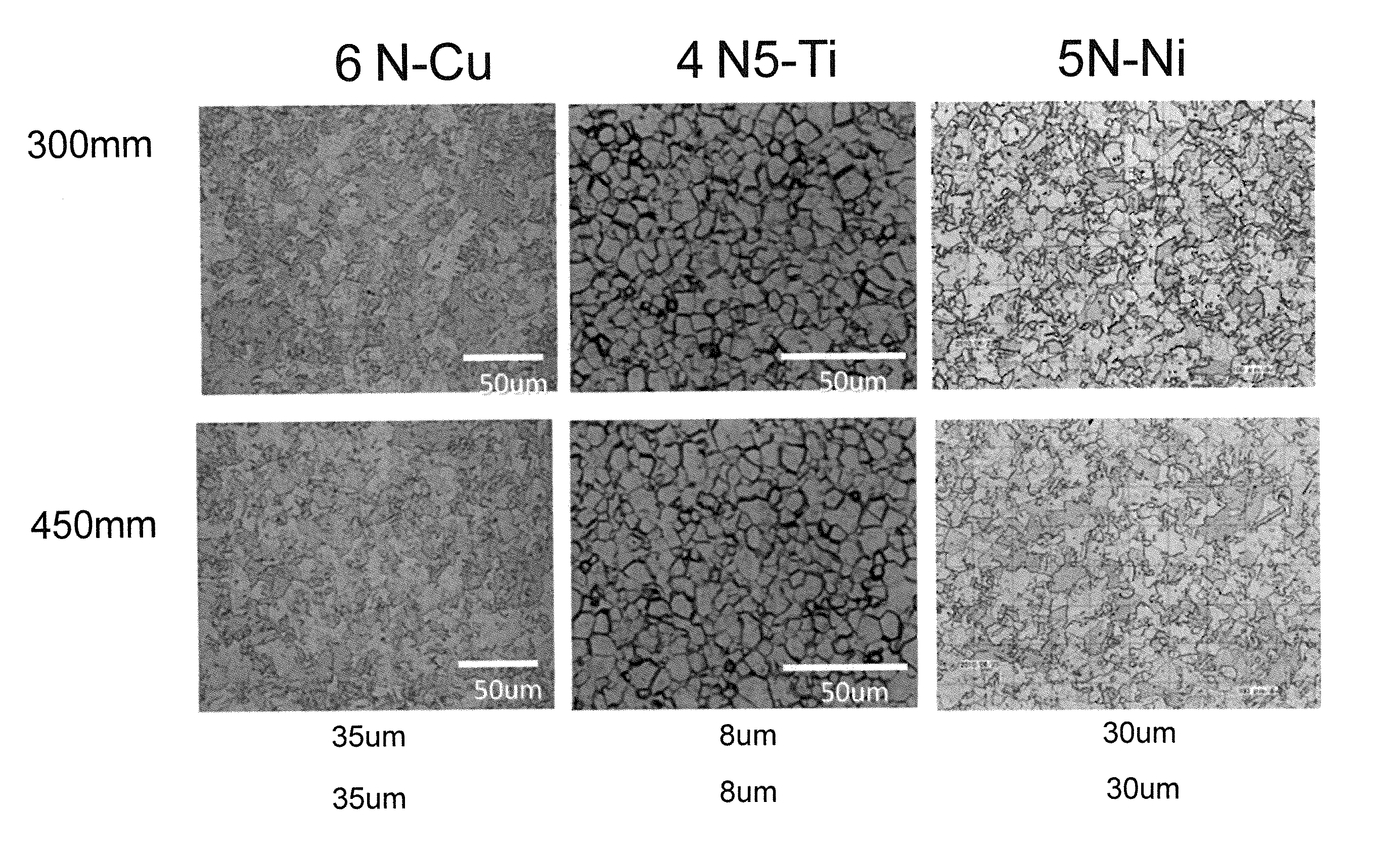
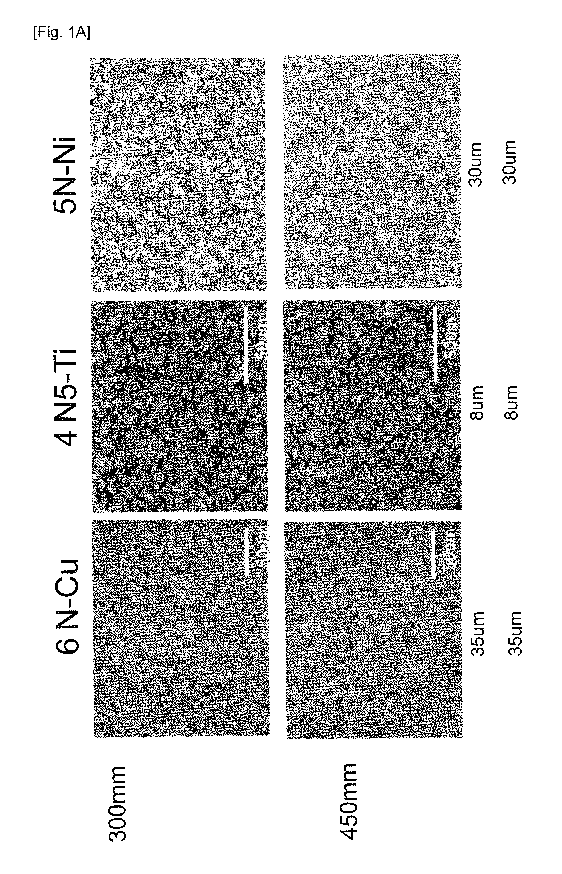
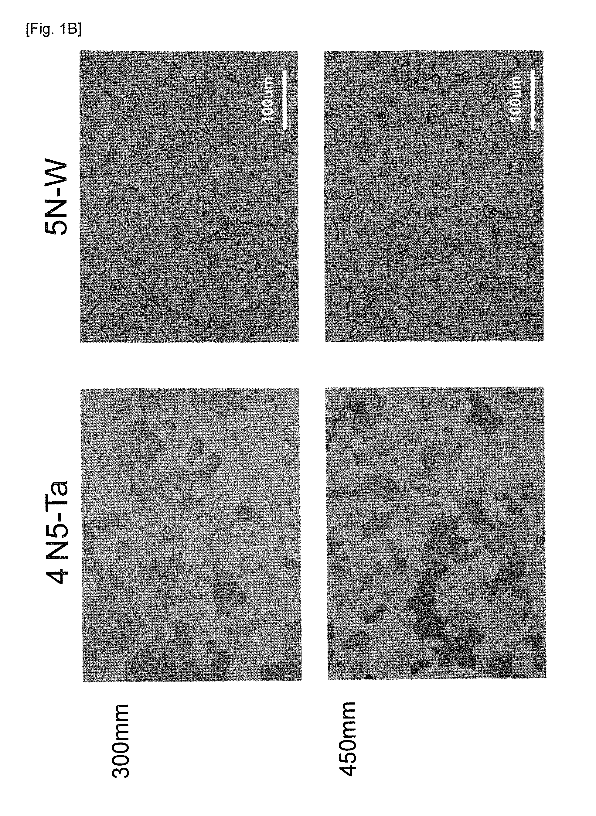
[0047]The present invention will be described based on Examples (experimental examples). Note that Examples are presented for merely illustrative purposes, and the present invention shall in no way be limited to these. That is, other aspects or modifications included in the present invention are encompassed.

(Production and Evaluation of Target for 450-mm Wafer)

[0048]In order to determine if the quality of a large-sized target is maintained, a Cu, a Ti, a Ta, a Ni, a Co and a W target of φ 600 mm were produced. For the production of targets, each ingot or powder of Purity 6N—Cu, 4N5-Ti, 4N5-Ta, 5N—Ni, 5N—Co and 5N—W was used as a starting material.

[0049]A manufacturing process of each material was coordinated according to the conditions used for producing a target for 300-mm.

[0050]Note that in order to control variations in crystal grain diameters, conditions in which a uniform processing strain was applied upon rolling, and heat treatment conditions which allowed uniform temperature...


PUM

PropertyMeasurementUnit
Temperatureaaaaaaaaaa
Lengthaaaaaaaaaa
Lengthaaaaaaaaaa

Abstract

Provided is a sputtering target-backing plate assembly for a 450-mm wafer, wherein the amount of warpage of the target developed during sputtering is 4 mm or less. Further provided is a method of manufacturing a sputtering target-backing plate assembly for a 450-mm wafer, the method comprising bonding a sputtering target material selected from copper, titanium, tantalum, nickel, cobalt, tungsten or alloys thereof with a backing plate made of copper, a copper alloy, an aluminum alloy, titanium or a titanium alloy at a temperature of 200 to 600° C., thereby the amount of warpage of the target developed during sputtering being 4 mm or less. An object of the present invention is to attempt to suppress detachment of a target from a backing plate and development of a crack by controlling development of warpage which occurs in a large sputtering target and to achieve uniform deposition properties.

Description

TECHNICAL FILED[0001]The present invention relates to a large sputtering target which can be adapted for a 450-mm wafer.BACKGROUND ART[0002]In manufacture of a semiconductor device, the costs for manufacturing an LSI Logic and a memory rapidly increase as a wiring width is becoming finer. The diameter of a wafer is required to be increased in accordance with the “Moore's law” in order to reduce the manufacturing cost thereof, and until now, increased diameters in every 10 years have brought innovation in the manufacturing technology.[0003]A large 450-mm wafer is a driving force for a new innovation, and semiconductor manufacturers, wafer manufacturers and various device manufacturers have started efforts for achieving 450 mm. The shape of a sputtering target is largely dependent on a design by sputtering equipment manufacturer. If a wafer diameter is increased from the current 300 mm to 450 mm, a sputtering target compatible with it is expected to be half again the diameter and twic...

Claims


Application Information

Patent Timeline
IPC IPC(8): C23C14/34B23K20/02B23K20/00B23K1/00
CPCC23C14/3414B23K20/002B23K20/02B23K1/0008C23C14/3407
Inventor SUZUKI, RYOOKABE, TAKEO
Owner JX NIPPON MINING& METALS CORP
Why Eureka
Try Eureka