Optical member with antireflection film, and method of manufacturing the same

a technology of anti-reflection film and optical member, which is applied in the field of optical member, can solve the problems of low productivity, inability to perform the sol-gel method in batch processing, and the patent literature 2 does not disclose the specific method of forming uneven thin films, so as to achieve high productivity, increase the choice of layers, and reduce the effect of materials

Inactive Publication Date: 2015-08-06
FUJIFILM CORP
View PDF2 Cites 20 Cited by
  • Summary
  • Abstract
  • Description
  • Claims
  • Application Information

AI Technical Summary

Benefits of technology

[0030]The optical member of the invention includes a transparent thin film layer, and a transparent fine uneven layer whose main component is an alumina hydrate, which are formed in this order on a surface of a transparent substrate, and the optical member includes at least a nitride layer or an oxynitride layer as the transparent thin film layer having an intermediate refractive index between the refractive index of the transparent substrate and the refractive index of the fine uneven layer. Use of a nitride allows providing a refractive index higher than that of an oxide layer, and this allows significantly increasing choices of the layer disposed between the transparent substrate and the fine uneven layer.
[0031]In the case where the optical member of the invention includes a plurality of nitride layers and / or oxynitride layers of the same constituent element, the refractive indices of the layers can be controlled by changing the amount of nitridation by using vapor deposition, which allows batch processing to achieve high productivity, and this allows forming the layers using fewer materials.

Problems solved by technology

However, sol-gel methods cannot be performed in batch processing and has a problem of low productivity.
However, as mentioned previously, Patent Literature 2 does not disclose the specific method for forming the uneven thin film.
In this case, however, at least three materials (Al2O3, SiO2, TiO2) are necessary and the number of evaporation hearths or the number of targets required for forming the films are necessary, resulting in a very complicated production method.

Method used


Image

  • Optical member with antireflection film, and method of manufacturing the same
  • Optical member with antireflection film, and method of manufacturing the same
  • Optical member with antireflection film, and method of manufacturing the same

Examples


example 1

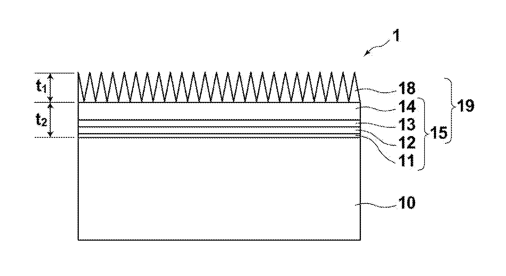
[0087]Using an ECR (electron cyclotron resonance) sputtering apparatus, a first SiON layer, a second SiON layer, a SiO2 layer, and an Al2O3 layer were formed in this order on a curved lens surface having a radius of curvature of 36.4 mm of a glass material OHARA S-LAH58 (having a refractive index nd=1.88300) with a maximum deposition angle φMax=62.5°. At this time, each layer was formed by ECR sputtering using Si and Al targets, respectively, with controlling the flow ratio of N2 to O2.

[0088]The first SiON layer (nd=1.75) had a film thickness of 80 nm, the second SiON layer (nd=1.61) had a film thickness of 80 nm, the SiO2 layer (nd=1.48) had a film thickness of 80 nm, and the Al2O3 layer had a film thickness of 30 nm. It should be noted that the film thickness here refers to the film thickness at the center portion of the lens, which is the largest thickness.

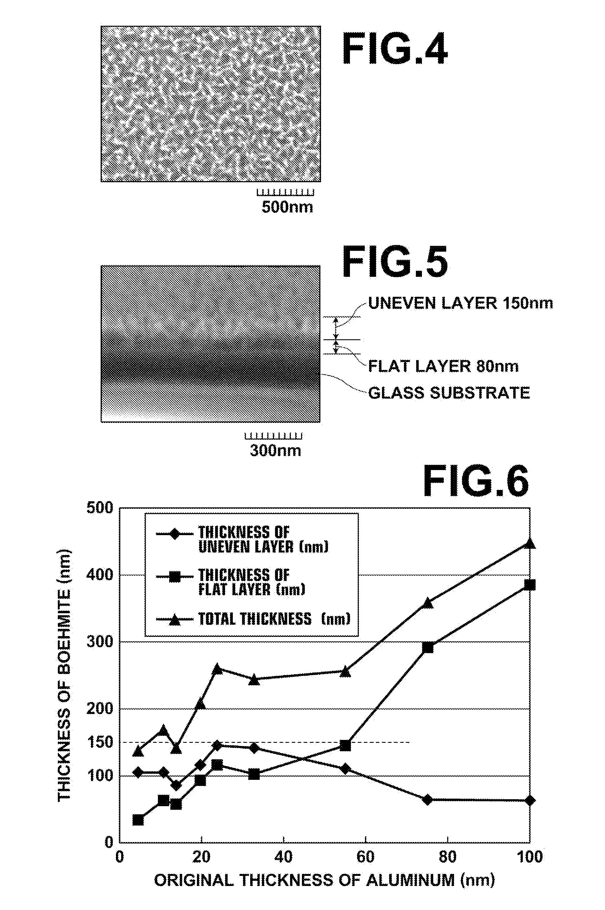
[0089]After the uppermost Al2O3 layer was formed, a hot water treatment was performed by immersing the layers in boiling wate...

example 2

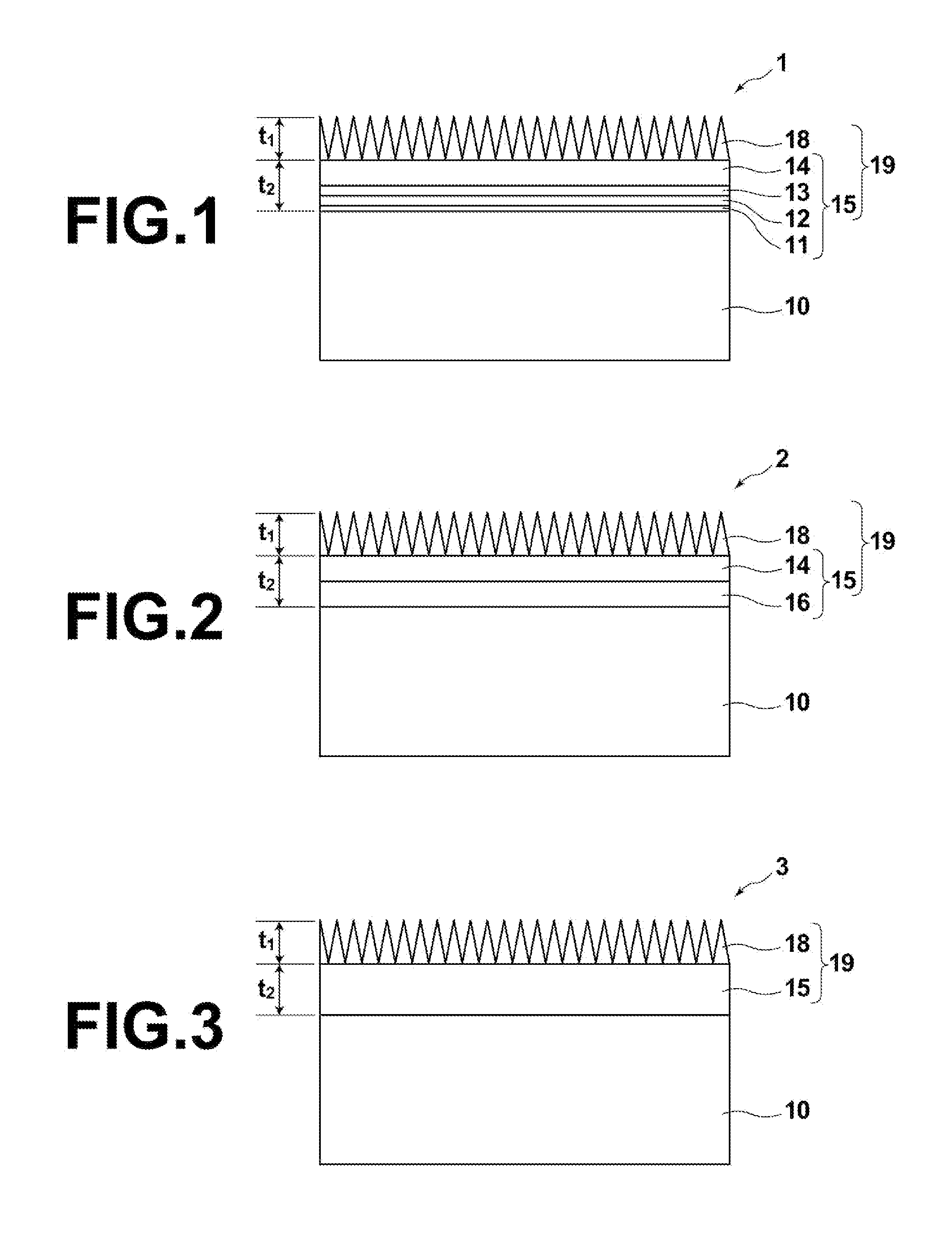
[0091]Using an ECR (electron cyclotron resonance) sputtering apparatus, an AIN layer, an AlON layer, a SiN layer, a first SiON layer, a second SiON layer, a SiO2 layer, and an Al2O3 layer were formed in this order on a curved lens surface having a radius of curvature of 36.4 mm of a glass material OHARA S-LAH58 (having a refractive index nd=1.88300) with a maximum deposition angle φMax=62.5°. At this time, each layer was formed by ECR sputtering using Si and Al targets, respectively, with controlling the flow ratio of N2 to O2.

[0092]The AIN layer (nd=2.01) had a film thickness of 40 nm, the AlON layer (refractive index nd=1.95) had a film thickness of 40 nm, the SiN layer (nd=1.91) had a film thickness of 40 nm, the first SiON layer (nd=1.64) had a film thickness of 40 nm, the second SiON layer (nd=1.55) had a film thickness of 40 nm, the SiO2 layer (nd=1.46) had a film thickness of 40 nm, and the Al2O3 layer had a film thickness of 30 nm.

[0093]After the uppermost Al2O3 layer was fo...


PUM

PropertyMeasurementUnit
thicknessaaaaaaaaaa
thicknessaaaaaaaaaa
thicknessaaaaaaaaaa

Abstract

An antireflection film including a transparent thin film layer, and a transparent fine uneven layer whose main component is an alumina hydrate, which layers are formed in this order on a surface of a transparent substrate, is provided. The transparent thin film layer has an intermediate refractive index between the refractive index of the transparent substrate and the refractive index of the fine uneven layer, and the transparent thin film layer includes at least a nitride layer or an oxynitride layer.

Description

CROSS-REFERENCE TO RELATED APPLICATIONS[0001]This application is a Continuation of PCT International Application No. PCT / JP2013 / 006048 filed on Oct. 10, 2013, which claims priority under 35 U.S.C. §119(a) to Japanese Patent Application No. 2012-229873 filed on Oct. 17, 2012. Each of the above applications is hereby expressly incorporated by reference, in its entirety, into the present application.BACKGROUND OF THE INVENTION[0002]1. Field of the Invention[0003]The present invention relates to an optical member and a method of manufacturing the optical member, and in particular to an optical member provided with an antireflection film on a surface thereof and a method of manufacturing the optical member.[0004]2. Description of the Related Art[0005]Conventionally, lenses (transparent substrates) made of a light-transmitting member, such as glass or plastic, are provided on the light entrance surface thereof with an antireflection structure (antireflection film) for reducing loss of the...

Claims


Application Information

Patent Timeline
Patent Type & Authority Applications(United States)
IPC IPC(8): G02B1/11C23C14/00
CPCG02B1/118C23C14/0036G02B1/11C03C2218/322C03C2217/734C03C2217/77C03C17/3435C23C14/0676C23C14/081C23C14/10C23C14/5846G02B1/115B32B9/00C03C17/34
Inventor SONODA, SHINICHIROHAKUTA, SHINYA
Owner FUJIFILM CORP
Why Eureka
Try Eureka