

Conductive optical device, input device, and display device
a conductive optical and input device technology, applied in the direction of metallic pattern materials, synthetic resin layered products, metal layered products, etc., can solve the problems of insufficient optical characteristics of proposed technology, affect the quality of display units and input units accordingly, etc., to achieve superior optical characteristics, increase the filling density of surface structures, and fabricate conductive optical devices efficiently in a short time
Inactive Publication Date: 2015-08-06
DEXERIALS CORP
View PDF6 Cites 17 Cited by
- Summary
- Abstract
- Description
- Claims
- Application Information
AI Technical Summary
Benefits of technology
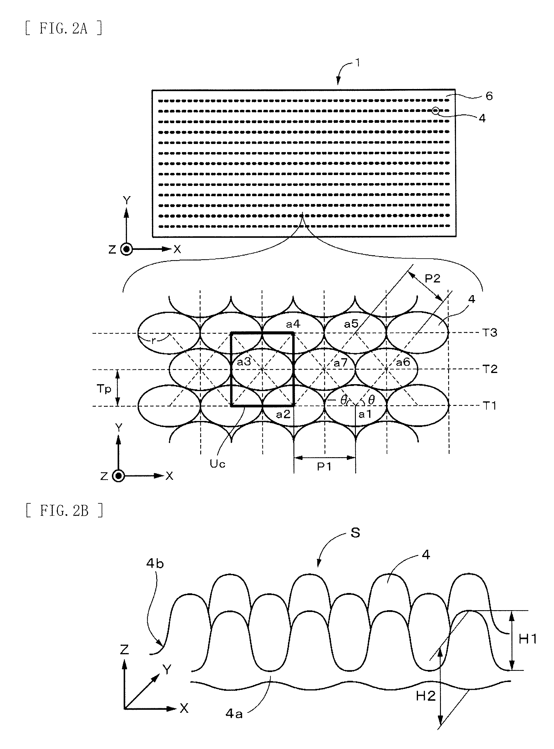
The technology described in this patent improves the filling rate of structures, such as optical devices, by making the arrangement pitch of the structures in the same track longer than the arrangement pitch of the structures between adjacent tracks. This results in better optical characteristics. In simpler terms, this technology helps create conductive optical devices with better optical performance.
Problems solved by technology
This may result in high reflectance depending on a thickness of the transparent conductive layer and impairment of quality of the display unit and the input unit accordingly.
However, the proposed technology is insufficient in optical characteristics.
Method used
View moreImage
Smart ImageViewing Examples

Examples
first embodiment (
1. First Embodiment (an example of a conductive optical device in which structures are arrayed in a hexagonal lattice pattern)
second embodiment (
2. Second Embodiment (an example of the conductive optical device in which the structures are arrayed in a tetragonal lattice pattern)
third embodiment (
3. Third Embodiment (an example of the conductive optical device in which the structures are provided on both surfaces)
Login to View More PUM
| Property | Measurement | Unit |
|---|---|---|
| conductive | aaaaa | aaaaa |
| wavelength | aaaaa | aaaaa |
| transparent conductive | aaaaa | aaaaa |
Abstract
A conductive optical device includes: a base; a plurality of structures supported by the base, and arranged at a pitch that is equal to or shorter than a wavelength of visible light; and a transparent conductive layer provided on a surface-side of the structures, and having a shape that follows along a surface shape of the structures. The following relational expressions are satisfied:y≧−1.785x+3.238y≦0.686where x is a refractive index and y is an aspect ratio, of each of the structures.
Description
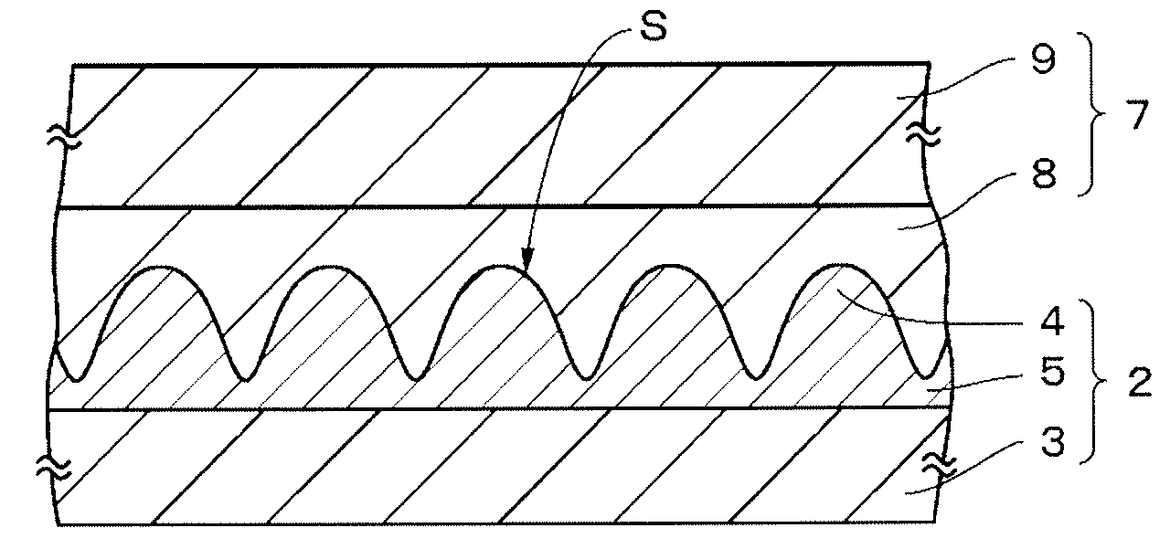
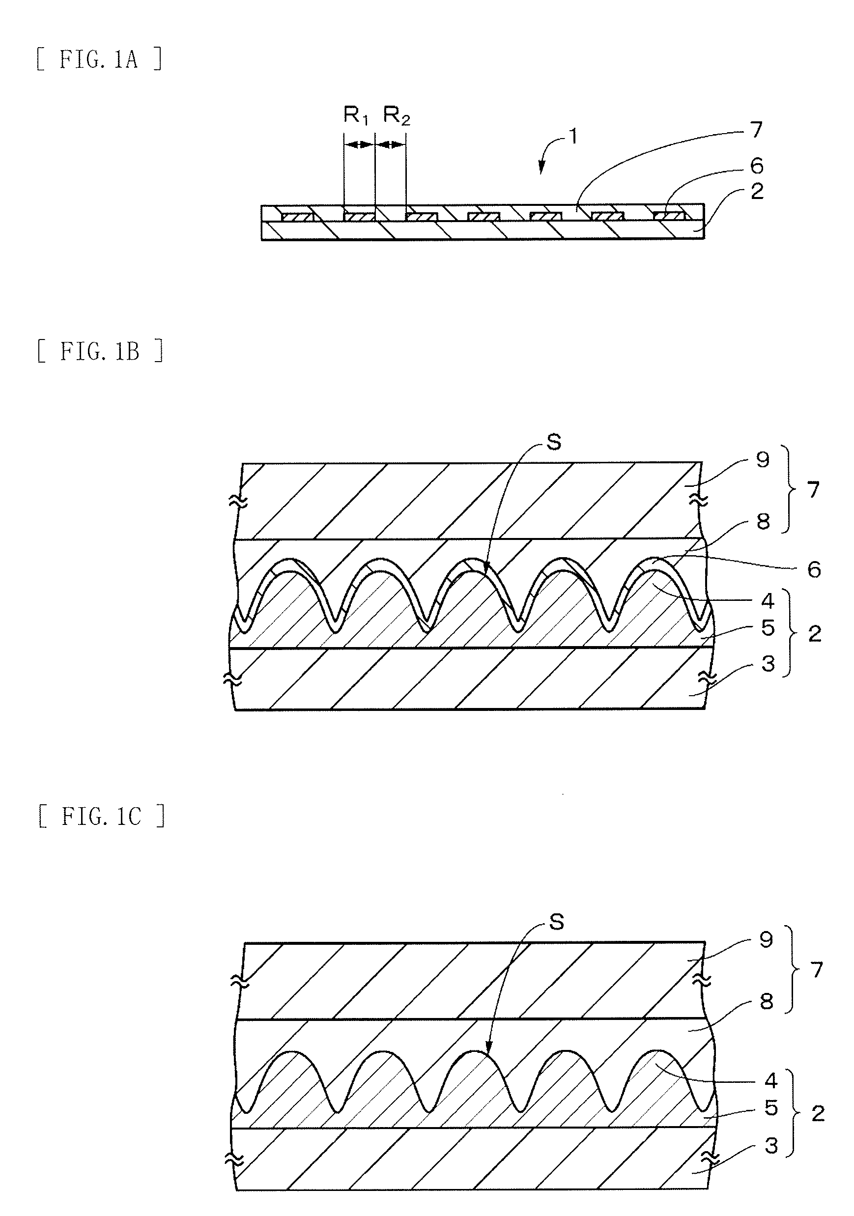
TECHNICAL FIELD[0001]The technology relates to a conductive optical device, to an input device, and to a display device. More specifically, the technology relates to a conductive optical device having an antireflection function.BACKGROUND ART[0002]A conductive optical device, in which a transparent conductive layer is formed on a planar surface of a base, is used for a display unit such as an electronic paper as well as for an input unit such as a touch panel. As a material of the transparent conductive layer used in the conductive optical device, a high refractive index material (such as ITO (Indium Tin Oxide)) is used. This may result in high reflectance depending on a thickness of the transparent conductive layer and impairment of quality of the display unit and the input unit accordingly.[0003]In order to improve transmission characteristics of the conductive optical device, a technology of forming an optical multilayer film is used. For example, Patent Document 1 proposes a con...
Claims
Login to View More Application Information
Patent Timeline
 Patent Type & AuthorityApplications(United States)
IPC IPC(8): H05K1/02G06F3/041G06F1/16H05K1/09G06F3/044G02B1/118G02B1/11G02B1/16G09F9/00
CPCB32B7/02G02B1/11C03C17/00G06F3/044G06F2203/04103H05K2201/0326H05K1/0284H05K1/0274G06F2203/04112G06F3/0412G06F1/16H05K1/09B32B9/005B32B15/20B32B27/08B32B27/30B32B27/325B32B27/34B32B27/36B32B27/365B32B27/38B32B27/40B32B3/28B32B2264/102B32B2307/3065B32B2307/412B32B2307/554B32B2457/00B32B2551/00G06F3/0446G06F3/0445
InventorENDOH, SOHMEIWADA, YUTAKAFUKUDA, TOMOO
OwnerDEXERIALS CORP