Method of soldering an electronic component with a high lateral accuracy

a technology of electronic components and lateral accuracy, which is applied in the direction of welding/cutting media/materials, manufacturing tools, and soldering apparatus, etc., can solve the problem of not allowing the exact positioning of electronic components, and achieve the effect of high positioning accuracy

Active Publication Date: 2015-08-06
LUMILEDS
View PDF0 Cites 7 Cited by
  • Summary
  • Abstract
  • Description
  • Claims
  • Application Information

AI Technical Summary

Benefits of technology

[0004]It is an object of the present invention to provide a method of soldering an electronic component to a subs

Problems solved by technology

When soldering electronic components to a substrate a problem arises in the field of optoelectronics or other applications in which the components need to be placed very accurate

Method used


Image

  • Method of soldering an electronic component with a high lateral accuracy
  • Method of soldering an electronic component with a high lateral accuracy

Examples


Embodiment Construction

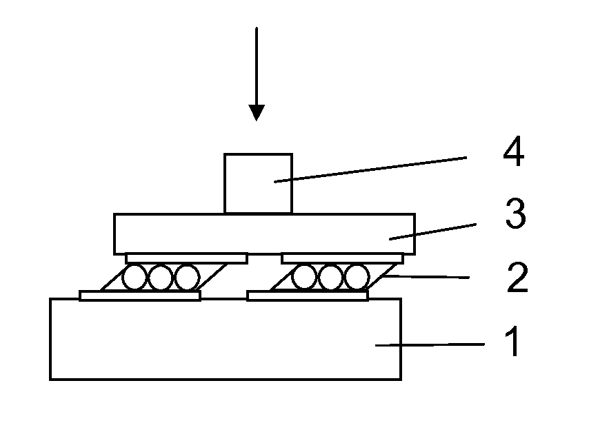
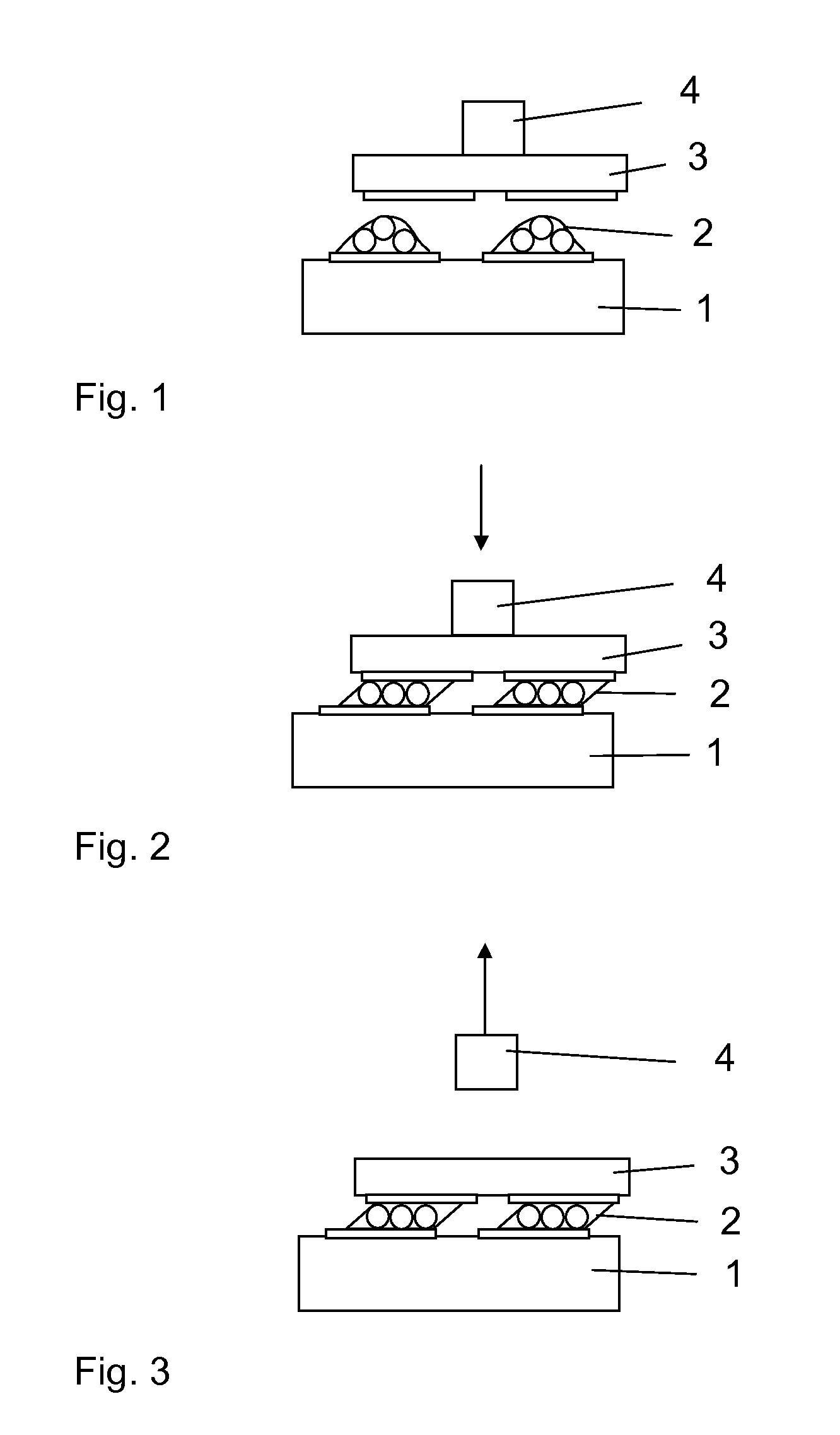
[0015]In the following the proposed method is described using a SnAgCu solder paste. The paste is prepared based on a commercially available SAC paste which typically contains 96 wt % Sn, 3.5 wt % Ag and 0.5 wt % Cu. To such a paste solid copper spheres having a diameter of 40 to 60 μm and optionally also small spheres with diameters between 10 and 25 μm are added. The proportion of the copper spheres is adjusted such that during reflow the copper spheres are still surrounded by a liquid Sn matrix (10 to 15% copper sphere volume, 35 to 40% SnAg volume and 50% flux volume).

[0016]The prepared solder paste 2 is printed on the board 1 to which the component 3 is to be soldered. The solder 2 is melted in the assembly machine at temperatures between 230° C. and 260° C. The component 3 is then positioned above the board 1 as indicated in FIG. 1. The component 1 is aligned to reference features (not shown in the figures) instead of the solder pads, in order to achieve the desired exact posi...


PUM

PropertyMeasurementUnit
Diameteraaaaaaaaaa
Diameteraaaaaaaaaa
Fractionaaaaaaaaaa

Abstract

The present invention relates to a method of soldering an electronic component (3) to a substrate (1) with high accuracy using transient liquid phase soldering. The component (3) is exactly positioned above the substrate (1) with a handling tool, placed in the melted solder (2) and pressed against the substrate (1). The component (3) is then released and the solder (2) allowed solidifying. Due to the use of a solder (2) having a sufficiently high amount of a second metal or metal alloy of a higher melting point which only partly dissolves in the melted first metal or metal alloy of a lower melting point, a solid framework forms during the liquid phase soldering which inhibits a lateral movement of the placed component (3) during soldering. Since the positioning of the component (3) is made using exact reference features on the substrate (1), the whole soldering process results in a highly accurate lateral position of the soldered component.

Description

TECHNICAL FIELD AND BACKGROUND[0001]The present invention relates to a method of soldering an electronic component to a substrate by transient liquid phase soldering, wherein a solder paste is deposited and melted on the substrate, the electronic component is placed in the melted solder by a handling tool and the melted solder is allowed to solidify.[0002]When soldering electronic components to a substrate a problem arises in the field of optoelectronics or other applications in which the components need to be placed very accurate on the substrate. For example, the optical center of light emitting surfaces of LEDs have to be positioned very accurate with respect to reference features of the substrate or board to enable cost effective and accurate assembly of a head lamp, i.e. assembly of the primary and secondary optics. In many applications PCB-boards (PCB: printed circuit board) are used as the substrate to which the electronic components have to be soldered. The tolerances of the...

Claims


Application Information

Patent Timeline
IPC IPC(8): H05K3/34B23K35/02C22C13/00B23K35/30C22C9/00B23K1/00B23K35/26
CPCB23K35/262H05K2203/04B23K35/0244B23K35/025C22C13/00H05K3/3463H05K3/3484C22C9/00H05K3/303H05K2201/10106H05K2203/0475B23K1/0016H05K3/3431B23K35/302B23K35/02H05K3/3485H01L24/81H01L2924/00011H01L2924/01322H01L2224/81805
Inventor ELGER, GORDON PATRICK RUDOLF
Owner LUMILEDS
Why Eureka
Try Eureka