Low-k dielectric layer with reduced dielectric constant and strengthened mechanical properties

a dielectric layer and low-k technology, applied in the field of low-k dielectric layers on substrates, can solve the problems of reducing the diffusion rate of porogens from the deposited layer, and reducing the mechanical strength of films, so as to improve mechanical properties, improve dielectric properties, and reduce the effect of k

Inactive Publication Date: 2015-08-20
APPLIED MATERIALS INC
View PDF2 Cites 16 Cited by
  • Summary
  • Abstract
  • Description
  • Claims
  • Application Information

AI Technical Summary

Benefits of technology

[0012]The present disclosure generally relates to dielectric layers used in integrated circuits. More specifically, the present disclosure describes a process and related apparatus for forming low-k d...

Problems solved by technology

However, cross-linking also reduces the rate of diffusion of porogenic materials from the deposited layer.
Thus, longer curing times become ineffective in removing the porogens to form additional pores.
It is also believed that the re...

Method used


Image

  • Low-k dielectric layer with reduced dielectric constant and strengthened mechanical properties
  • Low-k dielectric layer with reduced dielectric constant and strengthened mechanical properties
  • Low-k dielectric layer with reduced dielectric constant and strengthened mechanical properties

Examples


Embodiment Construction

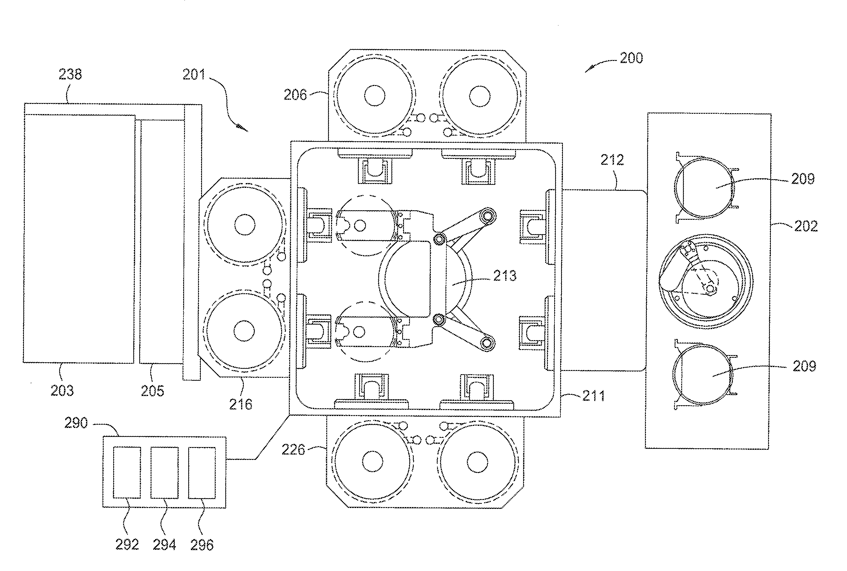
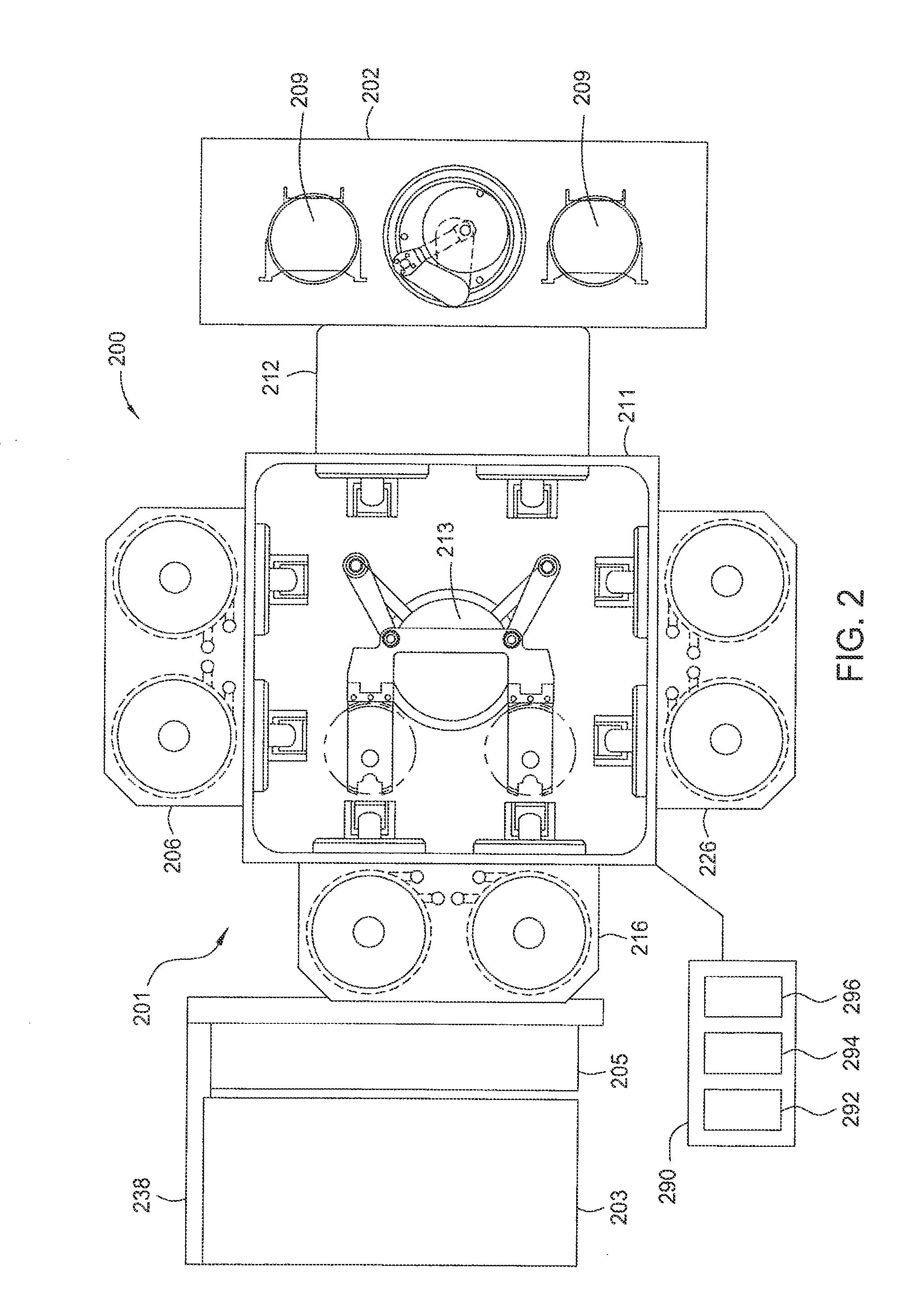
[0029]The present disclosure generally provides methods for forming a low-k dielectric layer within an integrated circuit (IC) device. However, it should be understood that the embodiments disclosed herein may have utility in system configurations other than those shown in the illustrative examples of the disclosure, and that these embodiments may also find applications which are not related to IC's, for example, micro-electro-mechanical systems (MEMS), displays and solar panels. Examples provided herein generally describe chemical vapor depositing and treating of low-k silicon-carbon oxide films, but the treating processes described herein can also be applied to porous low-k dielectric layers comprising other materials or produced by alternate means, such as spin-on glass (SOG).

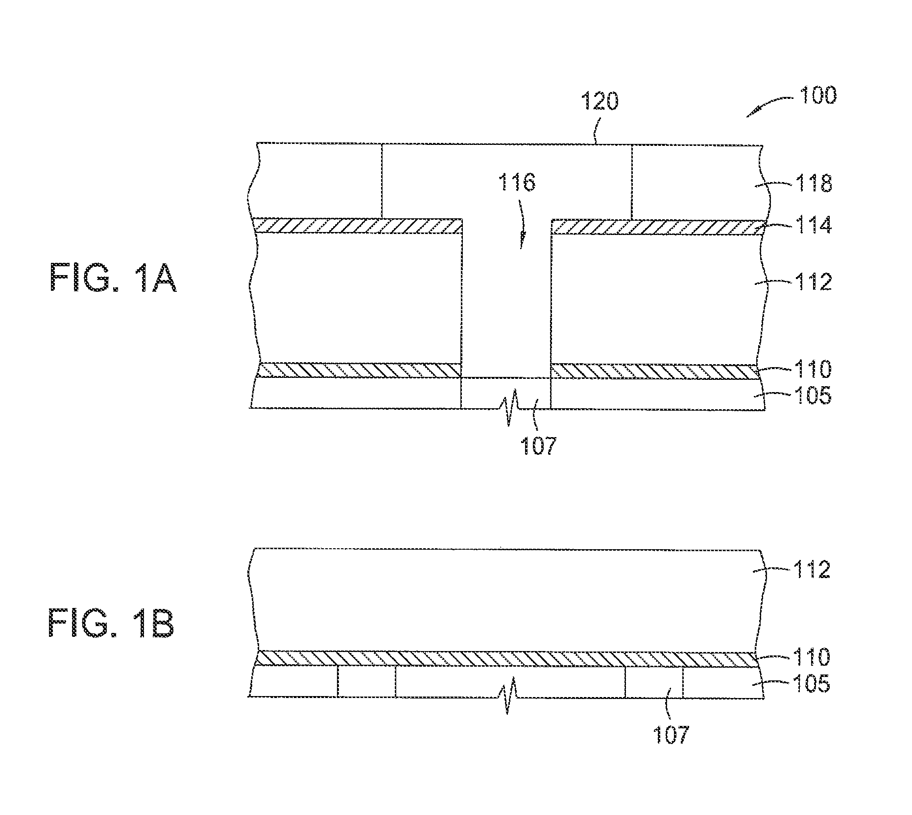
[0030]An example of a damascene structure which can be formed using the low-k layers described herein is shown in FIGS. 1A and 1B. A dielectric barrier layer 110 is formed on the substrate surface to elimina...


PUM

PropertyMeasurementUnit
Poweraaaaaaaaaa
Poweraaaaaaaaaa
Mechanical propertiesaaaaaaaaaa

Abstract

Embodiments of the present invention generally provide a method and apparatus for forming a low-k dielectric porous silicon oxycarbon layer within an integrated circuit. In one embodiment, a method is provided for depositing a porogen and bulk layer containing silicon oxycarbon layer, selectively removing the porogens from the formed layer without simultaneously cross-linking the bulk layer, and then cross-linking the bulk layer material. In other embodiments, methods are provided for depositing multiple silicon oxycarbon sublayers, selectively removing porogens from each sub-layer without simultaneously cross-linking the bulk material of the sub-layer, and separately cross-linking the sub-layers.

Description

CROSS-REFERENCE TO RELATED APPLICATIONS[0001]This application claims benefit of U.S. provisional patent application Ser. No. 61 / 941,400, filed Feb. 18, 2014, which is hereby incorporated herein by reference.BACKGROUND[0002]1. Field of the Invention[0003]Embodiments of the present disclosure generally relate to the process of fabricating integrated circuits on substrates. More specifically, embodiments of the present disclosure describe processes and related apparatus for depositing low-k dielectric layers onto substrates for manufacturing integrated circuit devices.[0004]2. Description of the Related Art[0005]For decades, the semiconductor industry has worked toward producing integrated circuits (IC's) that are smaller, faster, and containing more devices than the IC's formed previously. Reduction of dielectric constants in low-k insulating materials is part of this effort. Low-k materials are typically considered those which have a dielectric constant, or k, of less than 4. The con...

Claims


Application Information

Patent Timeline
IPC IPC(8): C23C16/48C23C16/46C23C16/30C23C16/50
CPCC23C16/401C23C16/505C23C16/56H01L21/02126H01L21/02203H01L21/02274H01L21/0234H01L21/02348
Inventor KIM, TAEWANYIM, KANG SUBDEMOS, ALEXANDROS T.
Owner APPLIED MATERIALS INC
Why Eureka
Try Eureka