High voltage gallium nitride based semiconductor device and manufacturing method of the same

a gallium nitride and semiconductor technology, applied in semiconductor devices, diodes, electrical devices, etc., can solve the problems of increasing manufacturing costs, unable to achieve high breakdown voltage, and enlarged devices, so as to prevent an increase in manufacturing costs and high voltage power

Inactive Publication Date: 2015-08-27
SUMITOMO CHEM CO LTD
View PDF6 Cites 7 Cited by
  • Summary
  • Abstract
  • Description
  • Claims
  • Application Information

AI Technical Summary

Benefits of technology

[0028]According to one embodiment of the invention, a high voltage gallium nitride based semiconductor device can be provided that is suitable as a high voltage power device while preventing an increase in a manufacturing cost.

Problems solved by technology

In case of the high voltage power device, as mentioned above, a high breakdown voltage cannot be achieved, if the electric field intensity in the junction surface is not be reduced and a breakdown phenomenon is not be prevented by suppressing the carrier concentration to be low at an area close to the junction surface.
However, when the carbon concentration is suppressed to be low, in most cases, a manufacturing cost is increased.
For example, when the growth pressure is heightened, it is needed to supply a large flow amount of gas at high speed in order to prevent a gas-phase reaction in a growth furnace, thus the device is enlarged in size and the manufacturing cost is increased.
In addition, when the growth speed is lowered, a time required for growth becomes longer, thus it directly results in an increase of the manufacturing cost.
Furthermore, when the ratio of V / III is enlarged for the purpose of suppressing the carbon concentration to be low without heightening the growth pressure and lowering the growth speed, it is needed to supply ammonia in an extremely large amount.
As ammonia, usually a liquefied gas type ammonia is used, but a vapor pressure of ammonia is low, thus for the purpose of increasing the supply volume, it is needed to considerably enlarge the ammonia supply equipment in size and a processing capability of an abatement equipment may become a problem.

Method used


Image

  • High voltage gallium nitride based semiconductor device and manufacturing method of the same
  • High voltage gallium nitride based semiconductor device and manufacturing method of the same
  • High voltage gallium nitride based semiconductor device and manufacturing method of the same

Examples


Embodiment Construction

[0034]The preferred embodiments according to the invention will be explained below.

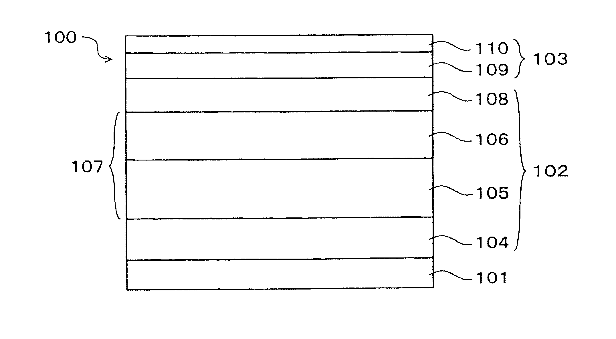
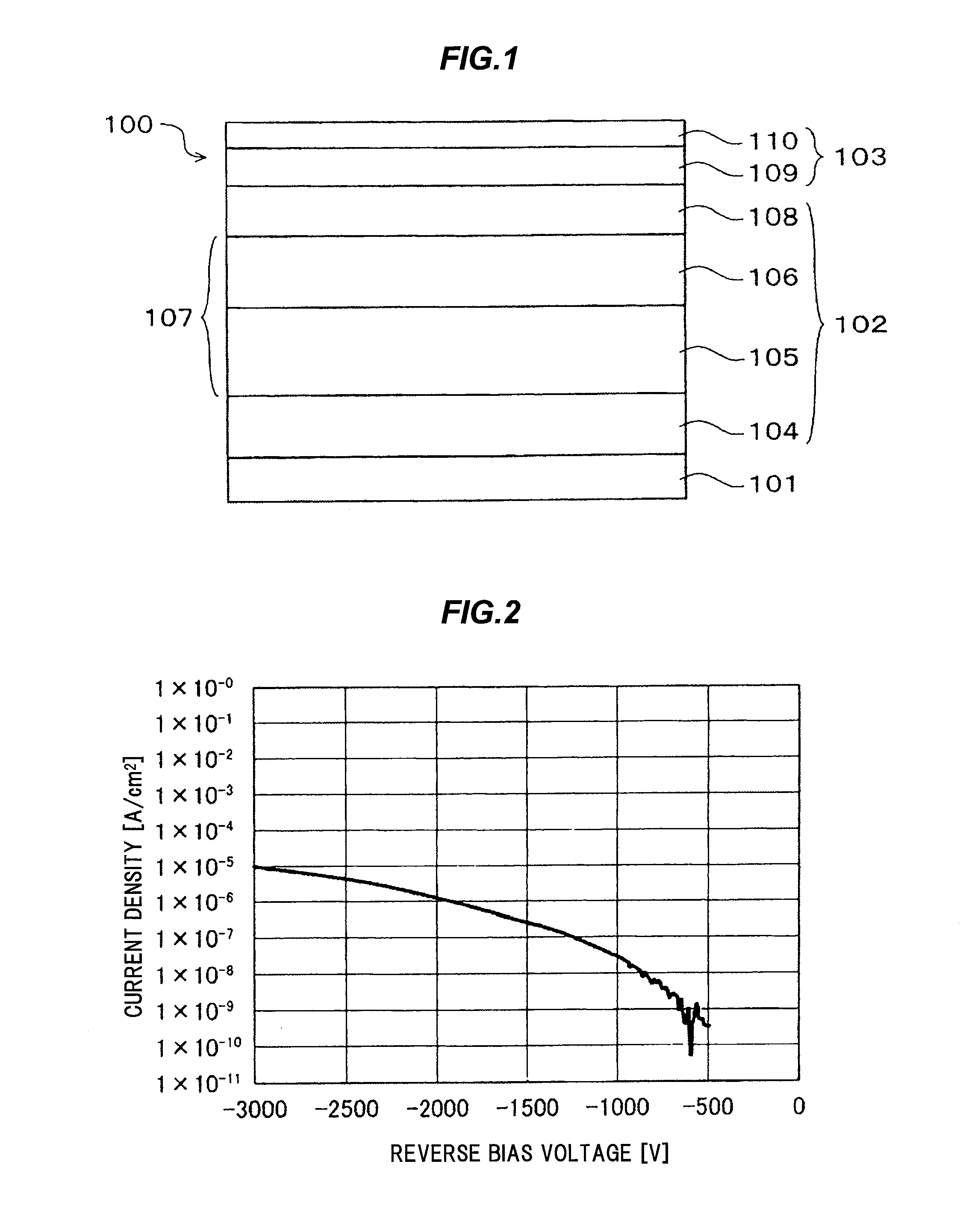
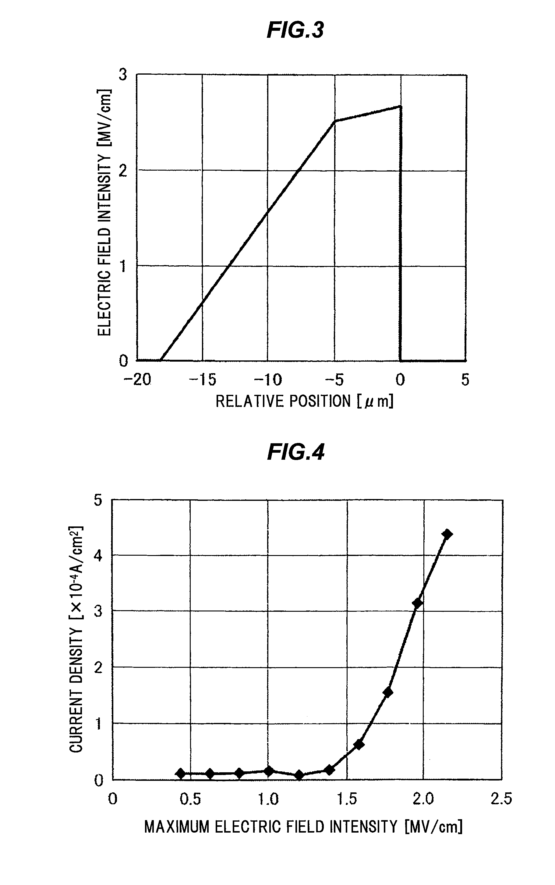
[0035]The high voltage gallium nitride based semiconductor device according to the embodiment includes an n-type gallium nitride freestanding substrate, and an n-type gallium nitride based semiconductor layer including a drift layer formed on the surface of the n-type gallium nitride freestanding substrate, so as to have a reverse breakdown voltage of not less than 3000 V, wherein the drift layer is configured such that a carbon concentration is not less than 3.0×10¹⁶ / cm3 in a region which has an electric field intensity of not more than 1.5 MV / cm when a maximum allowable voltage where there occurs no breakdown phenomenon is applied as a reverse bias voltage.

[0036]As the n-type gallium nitride freestanding substrate, for the purpose of preventing a leak current from being increased due to a dislocation that is a kind of a crystal defect and preventing a reverse breakdown voltage from being deteriorate...


PUM

PropertyMeasurementUnit
reverse breakdown voltageaaaaaaaaaa
electric field intensityaaaaaaaaaa
thicknessaaaaaaaaaa

Abstract

A high voltage gallium nitride based semiconductor device includes an n-type gallium nitride freestanding substrate, and an n-type gallium nitride based semiconductor layer including a drift layer formed on the surface of the n-type gallium nitride freestanding substrate so as to have a reverse breakdown voltage of not less than 3000 V. The drift layer is configured such that a carbon concentration is not less than 3.0×10¹⁶/cm3 in a region which has an electric field intensity of not more than 1.5 MV/cm when a maximum allowable voltage where there occurs no breakdown phenomenon is applied as a reverse bias voltage.

Description

[0001]The present application is based on Japanese patent application No. 2014-021246 filed on Feb. 6, 2014, the entire contents of which are incorporated herein by reference.BACKGROUND OF THE INVENTION[0002]1. Field of the Invention[0003]This invention relates to a high voltage gallium nitride based semiconductor device and a manufacturing method of the semiconductor device.[0004]2. Description of the Related Art[0005]A gallium nitride (GaN) based semiconductor is widely used all over the world as a material for an optical device represented by a light emitting diode (LED) and a laser diode (LD). Furthermore, the gallium nitride based semiconductor has extremely excellent physical properties of a material such as a wide band gap, a high electron mobility, a high saturation electron speed and a high breakdown voltage, thus in recent years, it is attracting attention also as a material of an electron material represented by a transistor, in particular, its application to a high volta...

Claims


Application Information

Patent Timeline
Patent Type & Authority Applications(United States)
IPC IPC(8): H01L29/20H01L21/02H01L29/10
CPCH01L29/207H01L29/66204H01L21/0254H01L29/2003H01L29/1095H01L21/02389H01L21/02576H01L21/02579H01L21/0262H01L29/36H01L29/66212H01L29/8611H01L29/872H01L29/73H01L29/74
Inventor KANEDA, NAOKI
Owner SUMITOMO CHEM CO LTD
Why Eureka
Try Eureka