Apparatus and Method for an Optical Waveguide Edge Coupler for Photonic Integrated Chips

Inactive Publication Date: 2015-10-01
HUAWEI TECH CO LTD
View PDF2 Cites 13 Cited by
  • Summary
  • Abstract
  • Description
  • Claims
  • Application Information

AI Technical Summary

Benefits of technology

[0005]In accordance with another embodiment, a method for fabricating a photonic chip includes placing a dielectric layer on a semiconductor substrate, and forming a semiconductor layer on the dielectric layer. A trench is then etched in the semiconductor layer and the dielectric layer. The trench has a width suitable to form a dielectric waveguide for fiber coupling, and has a bottom adjacent to a surface of the semiconductor substrate. The method further includes placing a low index dielectric layer at a bottom of the trench on the semiconductor substrate. The low index dielectric layer has smaller op

Problems solved by technology

A substantial MFD mismatch, referred to as a coupling mismatch, between the light propagating mode in silicon chip waveguide and the optical fiber causes significant loss of op

Method used


Image

  • Apparatus and Method for an Optical Waveguide Edge Coupler for Photonic Integrated Chips
  • Apparatus and Method for an Optical Waveguide Edge Coupler for Photonic Integrated Chips
  • Apparatus and Method for an Optical Waveguide Edge Coupler for Photonic Integrated Chips

Examples


Embodiment Construction

[0018]The making and using of the presently preferred embodiments are discussed in detail below. It should be appreciated, however, that the present invention provides many applicable inventive concepts that can be embodied in a wide variety of specific contexts. The specific embodiments discussed are merely illustrative of specific ways to make and use the invention, and do not limit the scope of the invention.

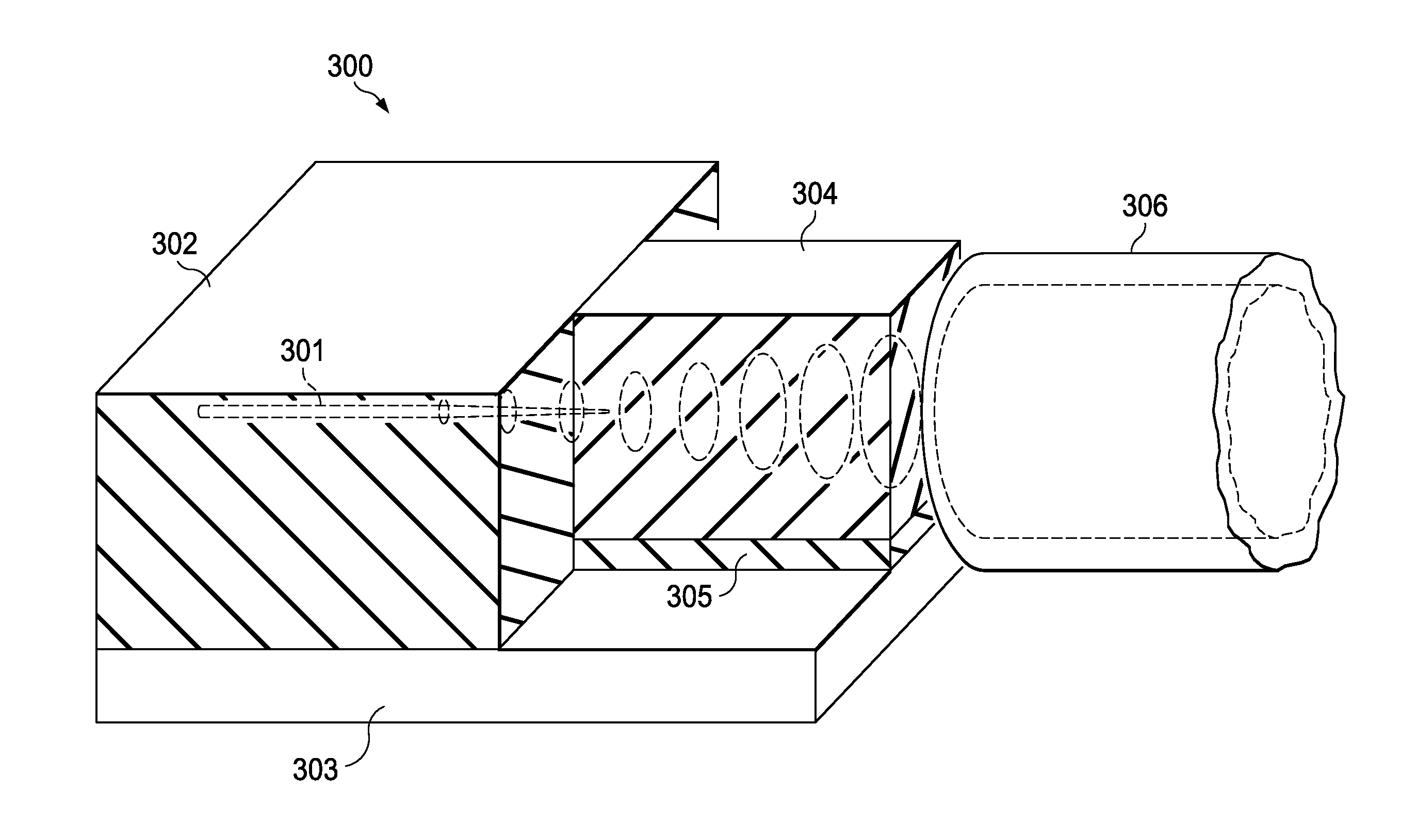
[0019]FIG. 1 shows a coupling mismatch scenario 100 between a silicon waveguide of a photonic chip and an optical fiber, e.g., a SMF28 type fiber. The nanowire is a silicon (Si) waveguide on a silicon oxide (SiO2) (in a chip) and has a cross section substantially smaller than the optical fiber. For example, the waveguide has a rectangular cross section with about a 500 nm width and about a 200 nm height. At the interface between the waveguide and the fiber, the MFD of the waveguide, for instance for the TE mode, is substantially smaller than that of the fiber, which is referr...


PUM


Abstract

Embodiments are provided for photonic chip waveguides with improved coupling efficiency to optical fibers. In an embodiment, a photonic chip comprises a semiconductor substrate, a dielectric layer on the substrate, and a tapered silicon or semiconductor waveguide embedded in the dielectric layer. The dielectric layer has lower optical refractive index than the tapered waveguide and serves as a cladding for the tapered waveguide. The chip further includes, on the substrate, a dielectric waveguide adjacent to the dielectric layer. The tip of the tapered waveguide is embedded in the dielectric waveguide. The dielectric waveguide serves to couple the tapered waveguide to an optical fiber, enlarge and better confine the light propagation mode from the taper waveguide to the fiber.

Description

TECHNICAL FIELD[0001]The present invention relates to photonic chips, and, in particular embodiments, to an apparatus and method for an optical waveguide edge coupler for photonic integrated chips.BACKGROUND[0002]Silicon nanophotonic chips, such as in silicon on insulator (SOI) platforms, typically include waveguide cross-sections in the sub-micron scale, are highly compact and comprise a high level of function integration. To implement silicon chips in optical communications networks, the optical light to / from the chips need to be coupled to optical fibers or other waveguides. The optical fibers typically have around a 10 micrometers (μm) mode field dimension (MFD). A substantial MFD mismatch, referred to as a coupling mismatch, between the light propagating mode in silicon chip waveguide and the optical fiber causes significant loss of optical power at this interface. The mismatch problem can significantly hinder the optical transmission efficiency. Various schemes have been explo...

Claims


Application Information

Patent Timeline
IPC IPC(8): G02B6/12G02B6/132G02B6/136
CPCG02B6/12G02B6/132G02B6/136G02B6/305G02B2006/12061G02B2006/12176G02B2006/12178
Inventor JIANG, JIAGOODWILL, DOMINIC JOHNBERNIER, ERIC
Owner HUAWEI TECH CO LTD
Why Eureka
Try Eureka