Solution-processed ultraviolet light detector based on p-n junctions of metal oxides

a technology of metal oxides and ultraviolet light detectors, applied in semiconductor/solid-state device manufacturing, electrical apparatus, semiconductor devices, etc., can solve problems such as prohibitive processing of commercial products

Inactive Publication Date: 2015-10-08
UNIV OF FLORIDA RES FOUNDATION INC
View PDF4 Cites 17 Cited by
  • Summary
  • Abstract
  • Description
  • Claims
  • Application Information

AI Technical Summary

Benefits of technology

[0007]An embodiment of the invention is directed to a method to prepare the UV detector, where a substrate covered with an electrode layer, a cathode, has a p-type polycrystalline metal oxide layer deposited thereon, to which an n-type nanoparticulate metal oxide layer is deposited, and, ultimately, a counter-electrode layer, an anode, is formed thereon. The p-type polycrystalline metal oxide layer is deposited by p...

Problems solved by technology

Conventional photodetectors for these applications are typically made in vacuum processing conditions that are incompatible with high throughput rather than i...

Method used


Image

  • Solution-processed ultraviolet light detector based on p-n junctions of metal oxides
  • Solution-processed ultraviolet light detector based on p-n junctions of metal oxides
  • Solution-processed ultraviolet light detector based on p-n junctions of metal oxides

Examples


Embodiment Construction

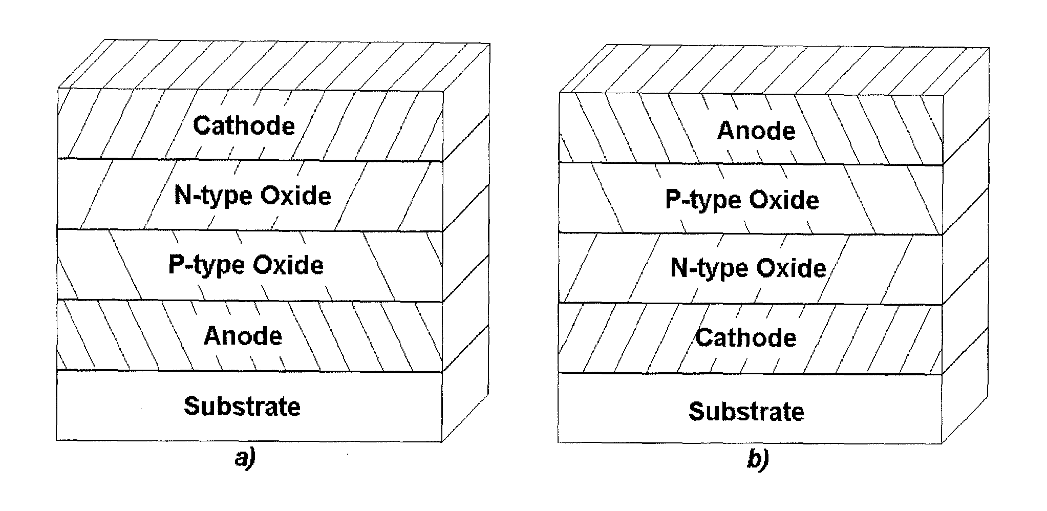
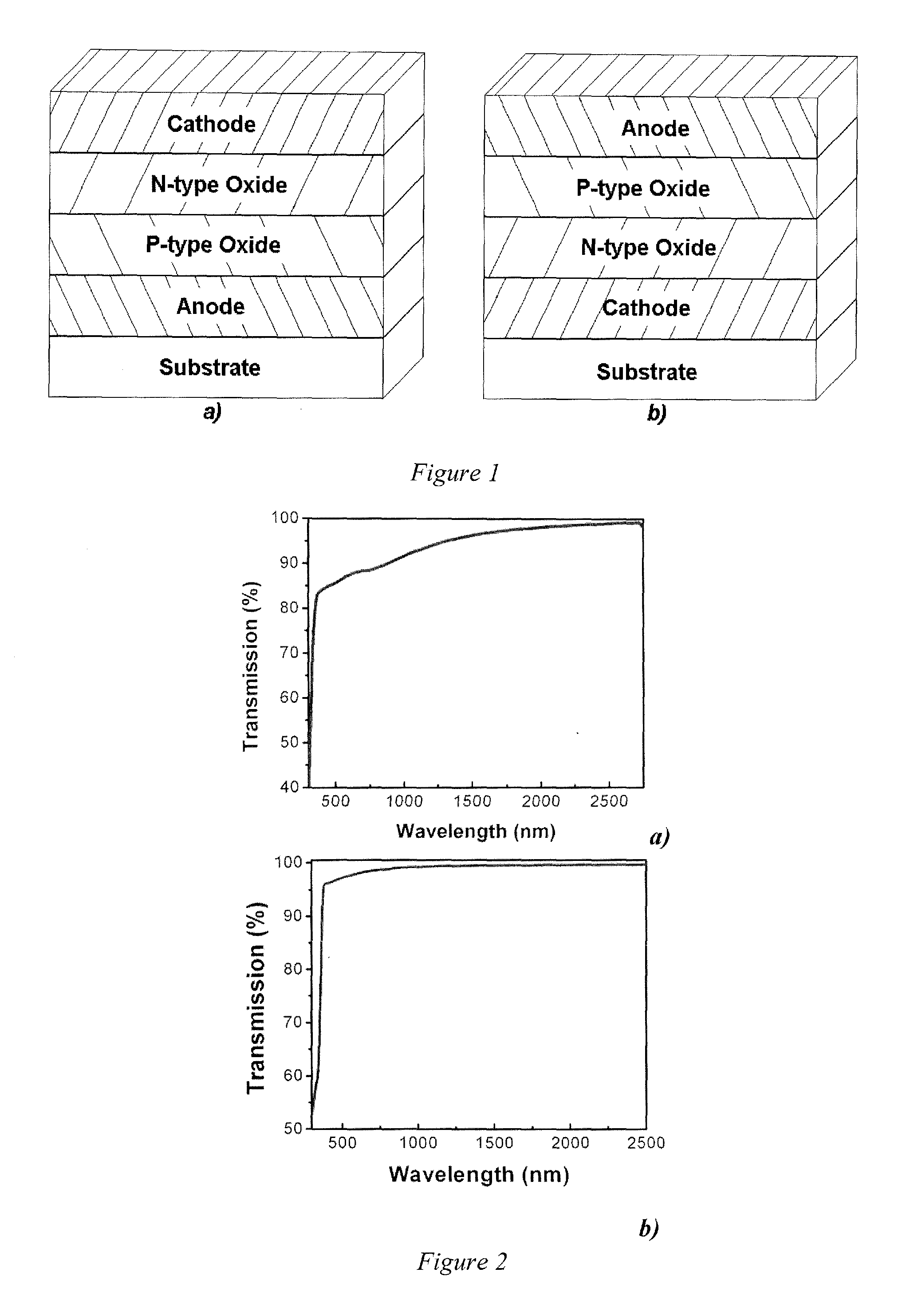
[0018]Embodiments of the invention are directed to a UV light detector comprising a pn-diode consisting of a p-type metal oxide, such as, NiO, Mn:SnO2, CuAlO2, CuGaO2, CuInO2, or SrCu2O2, and an n-type metal oxide, such as, ZnO, TiO2, MoO3, or V2O5, and to a method of forming the pn-junction of the wide-gap semiconductors layers that is fully solution-processed. In one embodiment of the invention, the UV light detector is constructed on any suitable substrate upon which an anode is deposited. Subsequently, nickel oxide or other p-type metal oxide is deposited as a layer on the anode, followed by deposition of zinc oxide, titanium dioxide, or other n-type metal oxide as a layer. The active portion of the UV detector is completed by deposition of a cathode on the n-type metal oxide. This “standard structure” is composed of layers to give a device structure of: substrate / anode / p-type oxide / n-type oxide / cathode. Alternatively, according to another embodiment of the invention, a UV detec...


PUM


Abstract

An ultraviolet light detector has a pn-junction of wide-gap semiconductors layers, where a p-type semiconductor layer with a polycrystalline metal oxide contacts an n-type semiconductor layer of metal oxide nanoparticles, or the converse. The ultraviolet detector is prepared using solvent based deposition methods and where temperatures can be maintained below 300° C.

Description

CROSS-REFERENCE TO RELATED APPLICATION[0001]The present application claims the benefit of U.S. Provisional Application Ser. No. 61 / 722,403, filed Nov. 5, 2012, which is hereby incorporated by reference herein in its entirety, including any figures, tables, or drawings.BACKGROUND OF INVENTION[0002]Ultraviolet (UV) light detectors are important devices with applications in a wide variety of fields of study and industries. Among the most prominent applications are solar-blind detectors, sensing for biologically damaging or biologically stimulating UV irradiation, detection of the presence or absence of the atmospheric UV-absorber ozone, and detection of UV light used for photolithography in semiconductor wafer manufacturing. Conventional photodetectors for these applications are typically made in vacuum processing conditions that are incompatible with high throughput rather than inexpensive fabrication techniques, such as, solution processing with flexible substrates. UV-detectors have...

Claims


Application Information

Patent Timeline
IPC IPC(8): H01L31/101H01L31/18H01L31/0352H01L31/109H01L31/032H01L31/0296
CPCH01L31/1016H01L31/032H01L31/0296H01L31/18H01L31/109H01L31/1828H01L31/035218
Inventor MANDERS, JESSE ROBERTKIM, DO YOUNGRYU, JIHOLEE, JAE WOONGSO, FRANKY
Owner UNIV OF FLORIDA RES FOUNDATION INC
Why Eureka
Try Eureka