Scatterometry-Based Imaging and Critical Dimension Metrology

a critical dimension and scattering technology, applied in the field of meteorological systems and methods, can solve the problems of difficult optical radiation penetration to the bottom layer, difficult characterization, and increased difficulty in characterization, and achieve the effect of improving the measurement performan

Active Publication Date: 2015-10-22
KLA TENCOR TECH CORP
View PDF1 Cites 124 Cited by
  • Summary
  • Abstract
  • Description
  • Claims
  • Application Information

AI Technical Summary

Benefits of technology

[0016]In a further aspect, the same scatterometry data acquired for CD metrology is used to calculate an image of the sample. In some examples, the image is a two dimensional (2-D) map of electron density, absorptivity, complex index of refraction, or a combination of these material characteristics. In some examples, the image is a three dimensional (3-D) map of electron density, absorptivity, complex index of refraction, or a combination of these material characteristics. The map is generated using relatively few physical constraints. The resulting map is generally unsuitable for measuring CD because it lacks sufficient resolution. However, the map is useful for debugging the wafer process when the sample geometry or materials deviate outside the range of expected values contemplated by the geometric model employed for CD measurement. In one example, the differences between the map and a rendering of the structure predicted by the geometric model according to its measured parameters are used to update the geometric model and improve its measurement performance.

Problems solved by technology

As devices (e.g., logic and memory devices) move toward smaller nanometer-scale dimensions, characterization becomes more difficult.
Devices incorporating complex three-dimensional geometry and materials with diverse physical properties contribute to characterization difficulty.
For example, modern memory structures are often high-aspect ratio, three-dimensional structures that make it difficult for optical radiation to penetrate to the bottom layers.
Optical metrology tools utilizing infrared to visible light can penetrate many layers of translucent materials, but longer wavelengths that provide good depth of penetration do not provide sufficient sensitivity to small anomalies.
As a result, the parameters characterizing the target often cannot be reliably decoupled with available measurements.
Optical radiation is often unable to penetrate layers constructed of these materials.
As a result, measurements with thin-film scatterometry tools such as ellipsometers or reflectometers are becoming increasingly challenging.
However, these approaches have not reliably overcome fundamental challenges associated with measurement of many advanced targets (e.g., complex 3D structures, structures smaller than 10 nm, structures employing opaque materials) and measurement applications (e.g., line edge roughness and line width roughness measurements).
Atomic force microscopes (AFM) and scanning-tunneling microscopes (STM) are able to achieve atomic resolution, but they can only probe the surface of the specimen.
In addition, AFM and STM microscopes require long scanning times.
Scanning electron microscopes (SEM) achieve intermediate resolution levels, but are unable to penetrate structures to sufficient depth.
Thus, high-aspect ratio holes are not characterized well.
In addition, the required charging of the specimen has an adverse effect on imaging performance.
Transmission electron microscopes (TEM) achieve high resolution levels and are able to probe arbitrary depths, but TEM requires destructive sectioning of the specimen.
However, the measurement model has limited degrees of freedom; typically much less than the degrees of freedom of the measured data.
If the actual sample is not accurately described by the measurement model, the resulting solution to the model based optimization does not provide any information concerning the source of the model mismatch.
This makes it very difficult to develop a measurement model that properly characterizes a specimen unless the structure of the specimen is well-known a priori.
This up-front knowledge of the specimen is often unavailable during process development
Future metrology applications present challenges for metrology due to increasingly small resolution requirements, multi-parameter correlation, increasingly complex geometric structures, and increasing use of opaque materials.
The resulting map is generally unsuitable for measuring CD because it lacks sufficient resolution.

Method used


Image

  • Scatterometry-Based Imaging and Critical Dimension Metrology
  • Scatterometry-Based Imaging and Critical Dimension Metrology
  • Scatterometry-Based Imaging and Critical Dimension Metrology

Examples


Embodiment Construction

[0026]Reference will now be made in detail to background examples and some embodiments of the invention, examples of which are illustrated in the accompanying drawings.

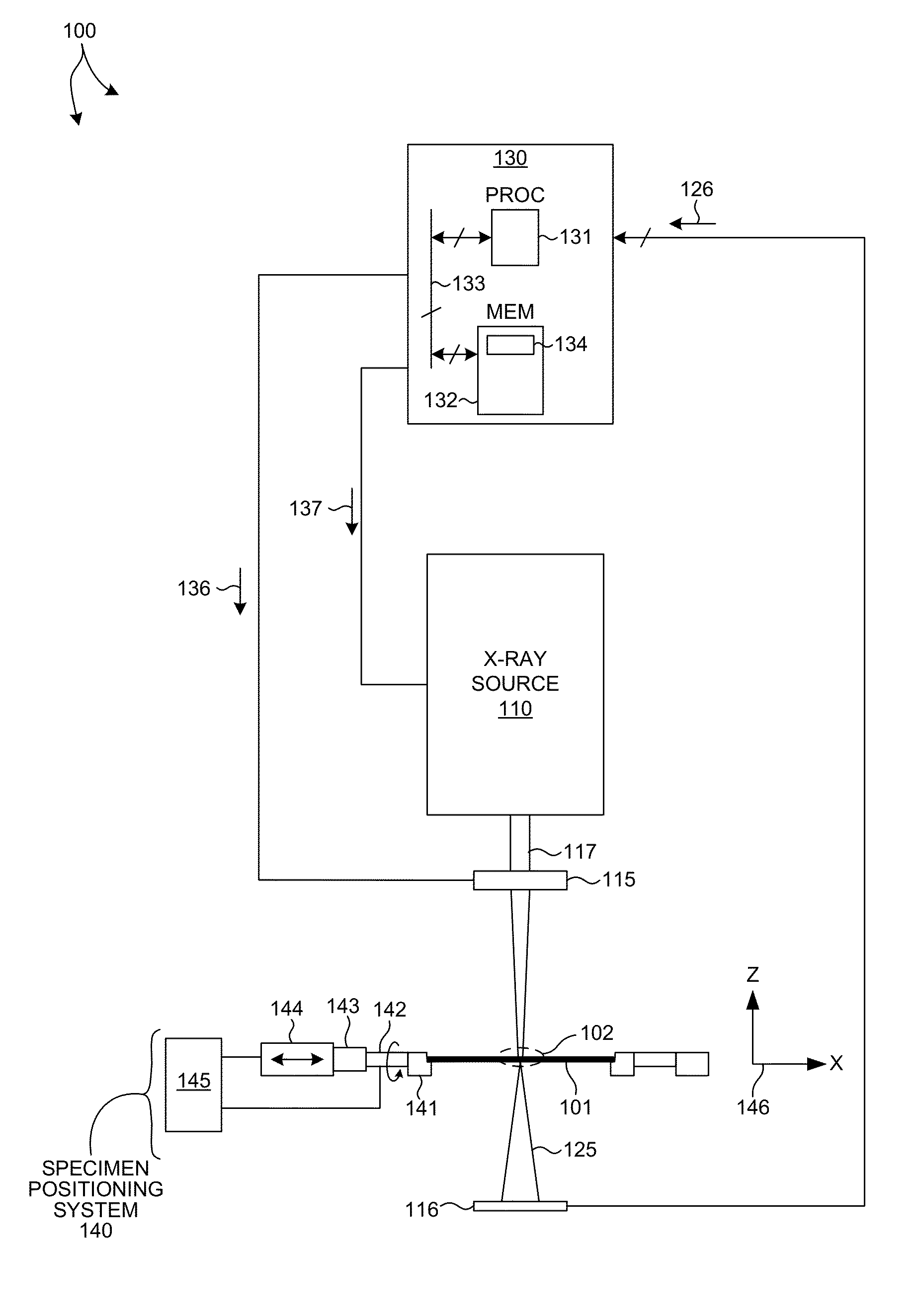
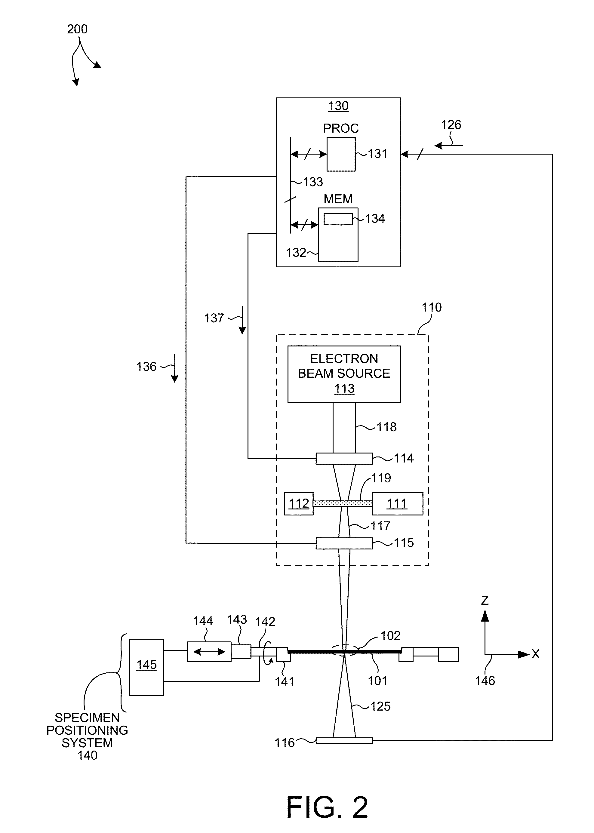
[0027]Methods and systems for performing measurements of semiconductor structures and materials based on scatterometry measurement data are presented. Such systems are employed to measure structural and material characteristics (e.g., material composition, dimensional characteristics of structures, etc.) associated with different semiconductor fabrication processes.

[0028]More specifically, scatterometry measurement data is used to generate an image of a measured structure based on the measured intensities of the detected diffraction orders. In some examples, the image is compared to structural characteristics estimated by a geometric, model-based parametric inversion of the same scatterometry measurement data. Discrepancies are used to update the geometric model of the measured structure and improve measurement perfor...


PUM

PropertyMeasurementUnit
roughnessaaaaaaaaaa
sizeaaaaaaaaaa
wavelengthsaaaaaaaaaa

Abstract

Methods and systems for performing measurements of semiconductor structures and materials based on scatterometry measurement data are presented. Scatterometry measurement data is used to generate an image of a material property of a measured structure based on the measured intensities of the detected diffraction orders. In some examples, a value of a parameter of interest is determined directly from the map of the material property of the measurement target. In some other examples, the image is compared to structural characteristics estimated by a geometric, model-based parametric inversion of the same measurement data. Discrepancies are used to update the geometric model of the measured structure and improve measurement performance. This enables a metrology system to converge on an accurate parametric measurement model when there are significant deviations between the actual shape of a manufactured structure subject to model-based measurement and the modeled shape of the structure.

Description

CROSS REFERENCE TO RELATED APPLICATION[0001]The present application for patent claims priority under 35 U.S.C. §119 from U.S. provisional patent application Ser. No. 61 / 982,183, entitled “X-Ray Imaging of Semiconductor Devices,” filed Apr. 21, 2014, and from U.S. provisional patent application Ser. No. 61 / 982,326, entitled “X-Ray Imaging of Semiconductor Devices,” filed Apr. 22, 2014, the subject matter of each is incorporated herein by reference in its entirety.TECHNICAL FIELD[0002]The described embodiments relate to metrology systems and methods, and more particularly to methods and systems for improved measurement accuracy.BACKGROUND INFORMATION[0003]Semiconductor devices such as logic and memory devices are typically fabricated by a sequence of processing steps applied to a specimen. The various features and multiple structural levels of the semiconductor devices are formed by these processing steps. For example, lithography among others is one semiconductor fabrication process ...

Claims


Application Information

Patent Timeline
Patent Type & Authority Applications(United States)
IPC IPC(8): G01N23/201
CPCG01N23/201G01N2223/611G01N2223/645H01L22/12G01N23/207
Inventor SEZGINER, ABDURRAHMANHENCH, JOHNBAKEMAN, MICHAEL S.
Owner KLA TENCOR TECH CORP
Why Eureka
Try Eureka