Ion implantation method and ion implantation apparatus
a technology of ion implantation and ion implantation, which is applied in the direction of optical radiation measurement, semiconductor/solid-state device testing/measurement, instruments, etc., can solve the problem of affecting the maintenance quality of semiconductor production
- Summary
- Abstract
- Description
- Claims
- Application Information
AI Technical Summary
Benefits of technology
Problems solved by technology
Method used
Image

Examples
modified example 1
[0099]FIGS. 13A and 13B are graphs illustrating examples of the correction control waveforms R1 and R2 according to the modified example and illustrating an example of the control waveform corresponding to the correction control waveform R illustrated in FIG. 8B. As in the correction control waveform R1 illustrated in FIG. 13A, the waveforms of the non-irradiation time t5 and the non-irradiation time t6 are not needed to be triangular waves and may be curves having an arbitrary shape. Further, as in the correction control waveform R2 illustrated in FIG. 13B, a voltage maybe fixed to the first voltage V1 (or −V1) for the non-irradiation time t5 and the non-irradiation time t6. In this case, the ion beam is located at the end of the irradiation area for the non-irradiation time t5 and the non-irradiation time t6 so that the scanning operation is temporarily stopped. Even in such a control waveform, the same effects as the above-described embodiments may be obtained. In a further modif...
modified example 2
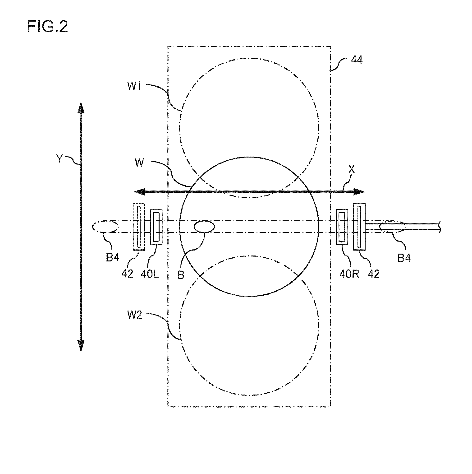
[0100]FIG. 14 is a graph illustrating an example of the correction control waveform R3 according to the modified example. In the control waveform illustrated in FIG. 14, a voltage is fixed to the fourth voltage V4 (or −V4) higher than the third voltage V3 (or −V3) for the non-irradiation time t5 and the non-irradiation time t6. Here, the third voltage V3 corresponds to a voltage in which the ion beam is located at the side measurement position C3 illustrated in FIG. 3, and the fourth voltage V4 corresponds to a voltage in which the ion beam is located at the scanning end position C4. In this way, since the ion beam is scanned so that the ion beam is located at the side measurement position C3, the ion irradiation amount per unit time may be measured by the side cups 40R and 40L even during the ion implantation processing. Accordingly, it is possible to handle a case where the ion irradiation amount per unit time changes during the ion implantation processing. Further, since the scan...
modified example 3
[0101]FIG. 15 is a graph illustrating examples of the correction control waveforms R4 and R5 according to the modified example. FIG. 15 schematically illustrates a method for adjusting the non-irradiation time by changing the scanning width in the non-irradiation area. The correction control waveform R4 of the period T4 indicated by the thin line and the correction control waveform R5 of the period T5 indicated by the thick line have the same waveform in the irradiation area. Further, the inclination dV / dt corresponding to a change value in time of the waveform in the non-irradiation area is the same, and the scanning speed in the non-irradiation area is the same. In such a condition, the scanning period is adjusted by changing the voltages AV1 and AV2 corresponding to the scanning width of the non-irradiation area. In this way, it is possible to adjust the scanning period only by changing the scanning width while the scanning speed in the non-irradiation area is constant. According...
PUM
 Abstract
Description
Claims
Application Information
 - Generate Ideas
- Intellectual Property
- Life Sciences
- Materials
- Tech Scout
- Unparalleled Data Quality
- Higher Quality Content
- 60% Fewer Hallucinations
Browse by: Latest US Patents, China's latest patents, Technical Efficacy Thesaurus, Application Domain, Technology Topic, Popular Technical Reports.
© 2025 PatSnap. All rights reserved.Legal|Privacy policy|Modern Slavery Act Transparency Statement|Sitemap|About US| Contact US: help@patsnap.com