Below a 1 mm thickness, it becomes difficult to manufacture any of these packages.
Accurate forming of leads to tight specifications and tolerances is problematic.
In extreme cases, manufacturing outside of specified tolerances can result in manufacturing interruptions, triggering financial penalties, vendor disqualifications and even litigation.
Poor control of lead bending in manufacturing is not the only limitation of these packages.
Because package height is a major consideration in IC packages, the leadframe is limited in thickness, typically to 200 μm or less, and it therefore exhibits relatively poor power dissipation capability because of the inability to effectively spread heat from a die into the
printed circuit board or
heat sink.
Such damage can result in yield loss during
visual inspection, and uncaught, can result in reliability failures.
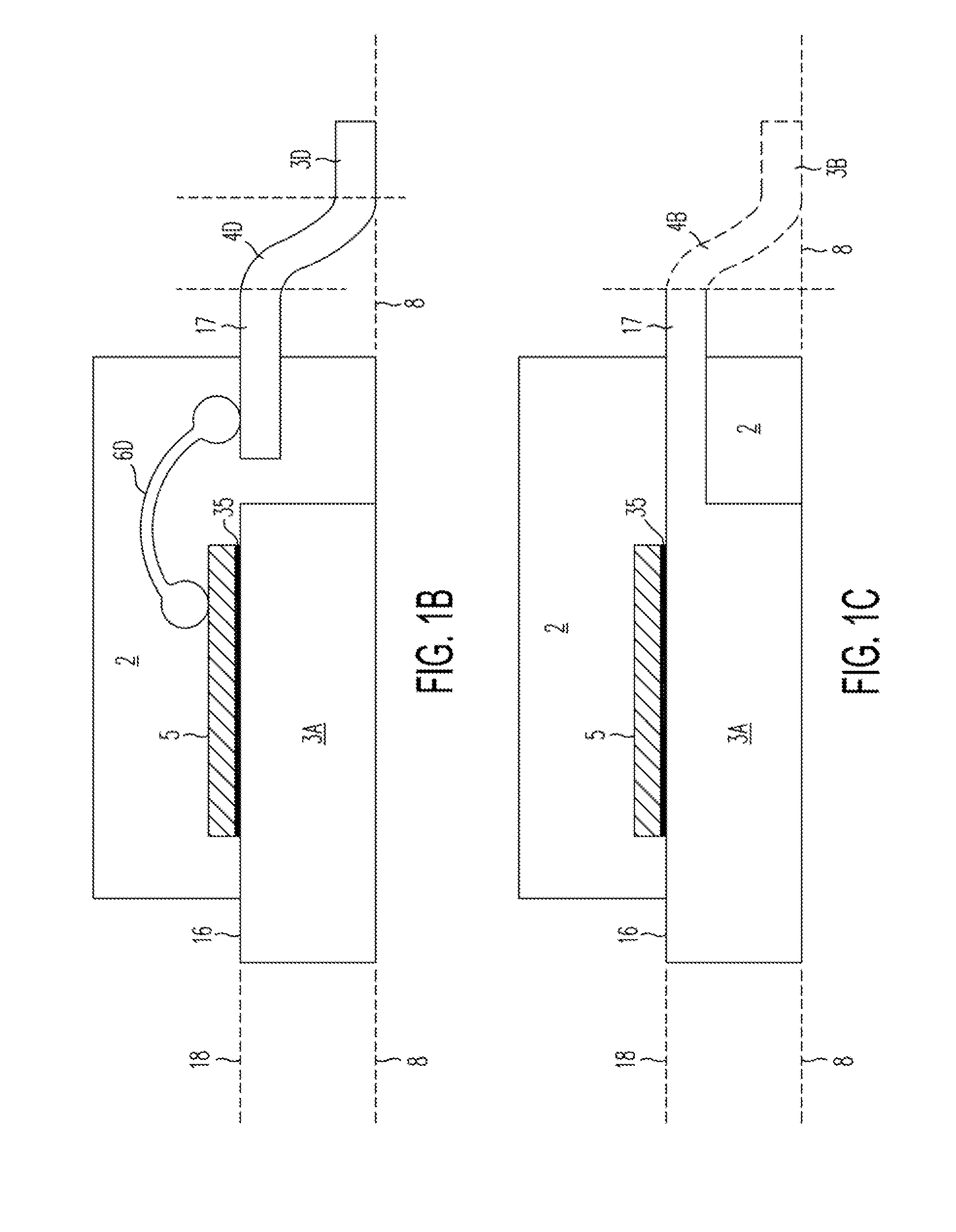
Another source of manufacturing defect can occur if bent portion 4D is bent too much or too little so that the bottom portion of conductive lead 3D is not coplanar with the planar bottom surface 8 of die pad 3A.
Because of its poor area efficiency, this package technology is therefore incompatible with space-sensitive applications such as smartphones and mobile personal
electronics.
Such a manual method of placing solder is slow and expensive, and therefore cost effective when used for only for few components.
While such a solder joint may be adequate for carrying the rated current of a
power component, it does not insure a low
thermal resistance between die pad 3A and PCB conductor 41B, 42, and 43B.
As such, the use of
solder paste 45 in wave solder manufacturing remains unavoidable when power components are mixed with other ICs.
An alternative PCB
assembly method, known as reflow manufacturing, involves printing
solder paste across the entire
printed circuit board before mounting the components, but this process, while very precise, is slow and therefore expensive, especially since high cost reflow ovens are required to melt the solder in a controlled manner to avoid movement of the components from floating during
soldering.
In circuit operation, however, stray source
inductance is problematic and much worse than drain
inductance.
As the source
voltage oscillates, the gate-to source
voltage may rise and fall above the
MOSFET's
threshold voltage, turning it on and off multiple times and increasing the switching loss accordingly.
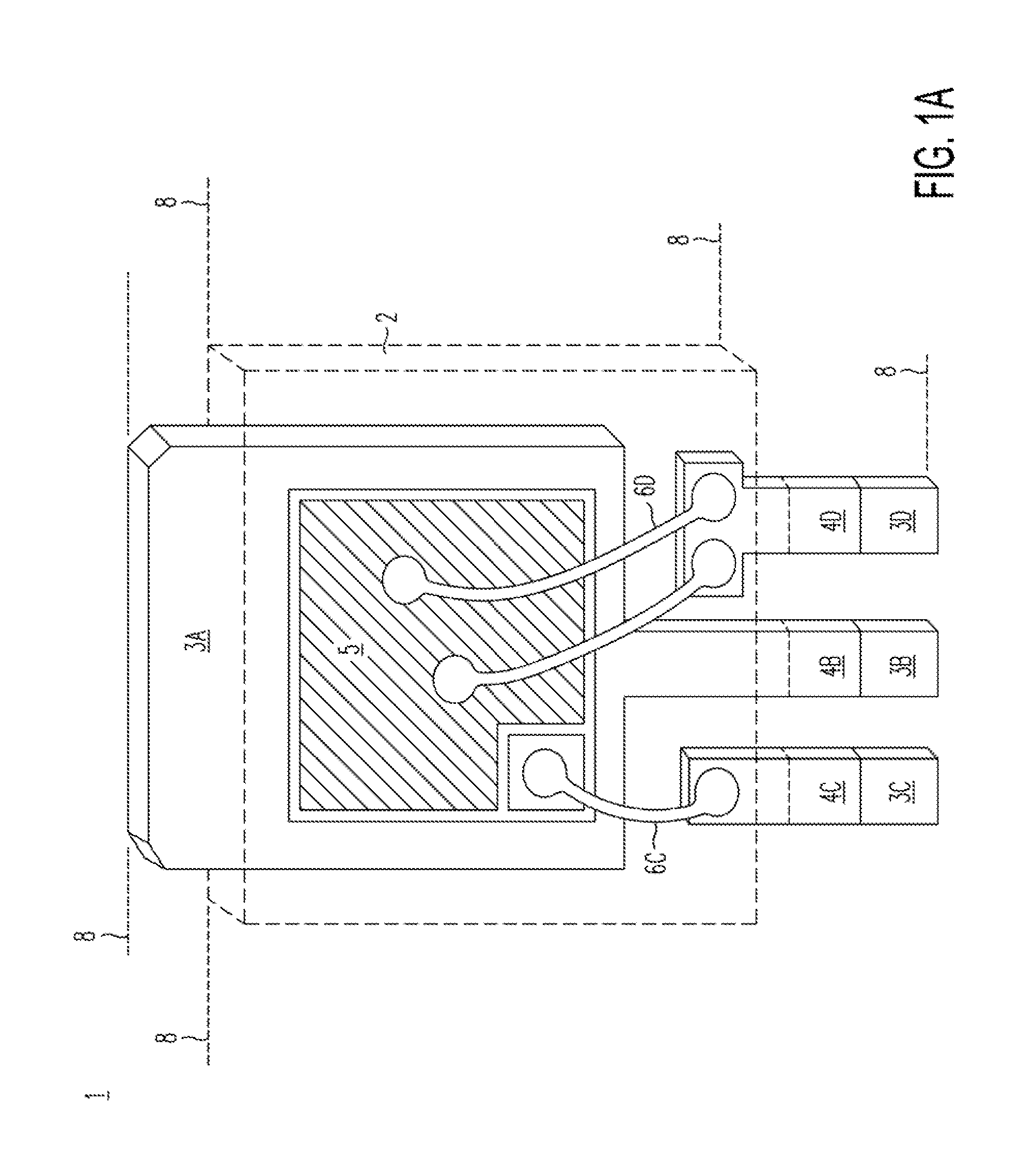
Unfortunately, such a conductive lead is not possible in
present day DPAK and D2PAK packages because conductive lead 3B is used for mechanical support during assembly and necessarily must be tied to die pad 3A.
Each and any change in the leadframe
pitch or package
size change requires a new mold to be fabricated, an expensive component requiring involving precision-machined steel molds.
Newer generation mold machines are even more expensive, even double in price.
Moreover, whenever the leadframe and cavity width or
pitch of a package is changed, other equipment such as trim and form machines must be modified adding an additional expense of $70,000 USD or more to accommodate the new package form factor.
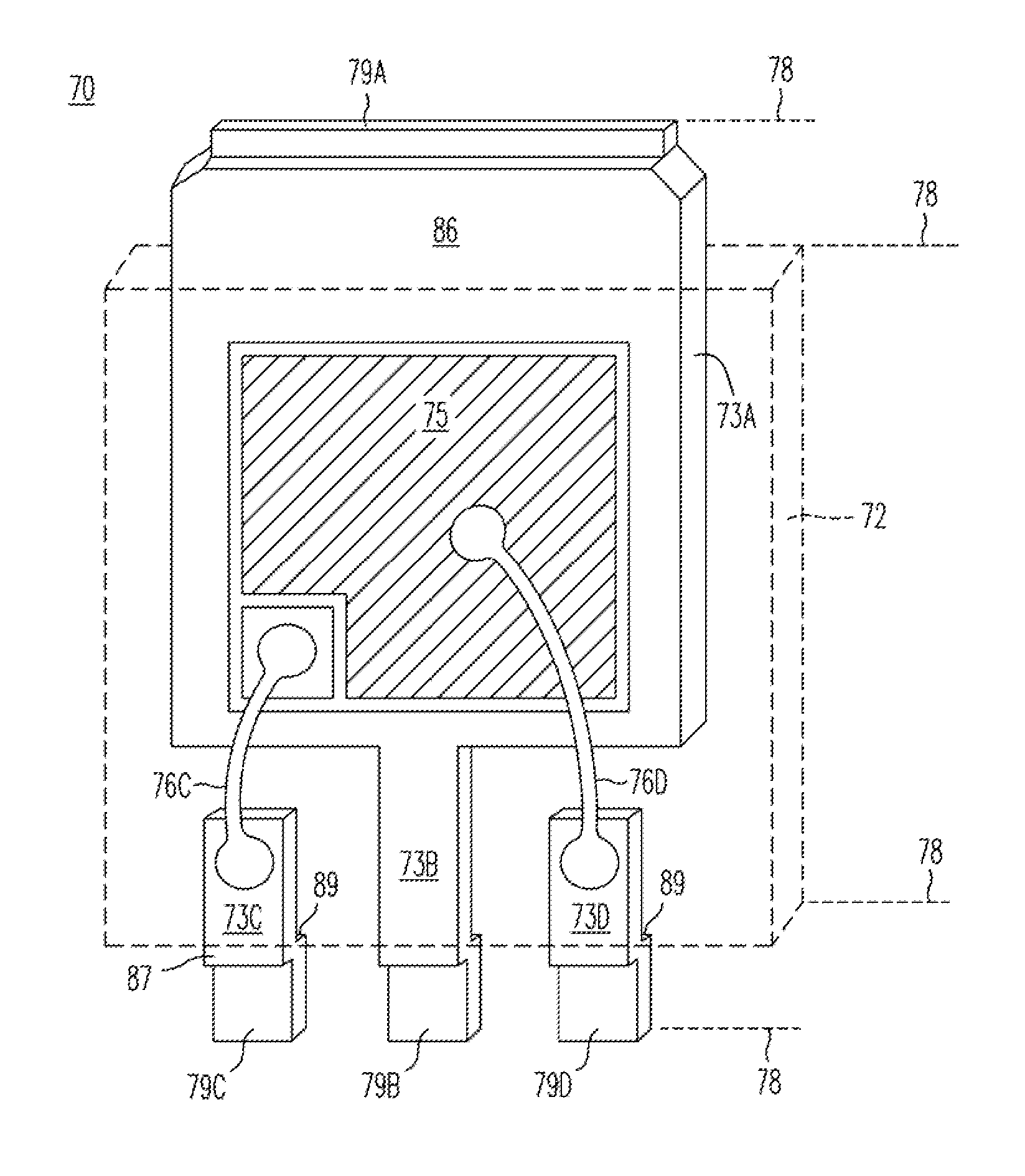
But since, as described previously, the die pad is necessarily tied to the center conductive lead, these standardized packages can only accommodate up to three separate electrical connections.
Because the main current flows through two bond wires instead of only one bond wire, as in the case of vertical devices, the packaging of lateral devices unavoidably suffers from higher parasitic package, i.e. wire, resistance.
In summary, today's high volume power packages had seen little advancement since their inception decades ago.
Factory lines for DPAK and D2PAK packages are inflexible, requiring large expenses to accommodate multiple package types.
The packages intrinsically are limited to a maximum of three electrical terminals, limiting their applicability to only a few device types.
The package's center conductive lead is necessarily shorted to the die pad, further limiting
layout options for a
semiconductor device.
The packages are area-inefficient, with large “keep out” zones and long conductive leads necessary to facilitate lead bending without damaging the molded plastic encapsulant.
The large package dimensions and long bond wires contribute to undesirable parasitic resistance and
inductance.
Lead bending is imprecise, making it difficult to insure good co-planarity of the leads with the bottom of the exposed die pad and adversely impacting PCB assembly yield.
And with all the forgoing limitations, the possibility to enhance today's power
package design and
manufacturing capability to accommodate low profile or multi-lead packages remains problematic both technically and economically.

