Virtual cell model geometry compression

a virtual cell model and geometry compression technology, applied in the field of semiconductor circuit design, can solve problems such as requiring attention, a potential issue or failure, and a complex drc tool, and achieve the effects of simplifying the geometric shape of the vhl, reducing the number of corners, and reducing the siz

Active Publication Date: 2015-11-26
SYNOPSYS INC
View PDF13 Cites 13 Cited by
  • Summary
  • Abstract
  • Description
  • Claims
  • Application Information

AI Technical Summary

Benefits of technology

[0006]Virtual cell model geometry compression is used to reduce the size of virtual hierarchical layer (VHL) data structures, and related data structures such as context data, which is used for physical verification of an integrated circuit design. A geometric shape in the VHL is simplified by reducing the number of corners it contains. Reducing the number of corners of a geo

Problems solved by technology

If the design violates the DRM in a certain location, the location represents a potential issue or failing requiring attention before manufacturing can commence.
The semiconductor process has grown in complexity such that a physical design layout must adhere to thousands of design rules before a design can be successfully fabricated a

Method used


Image

  • Virtual cell model geometry compression
  • Virtual cell model geometry compression
  • Virtual cell model geometry compression

Examples


Embodiment Construction

Configuration Overview

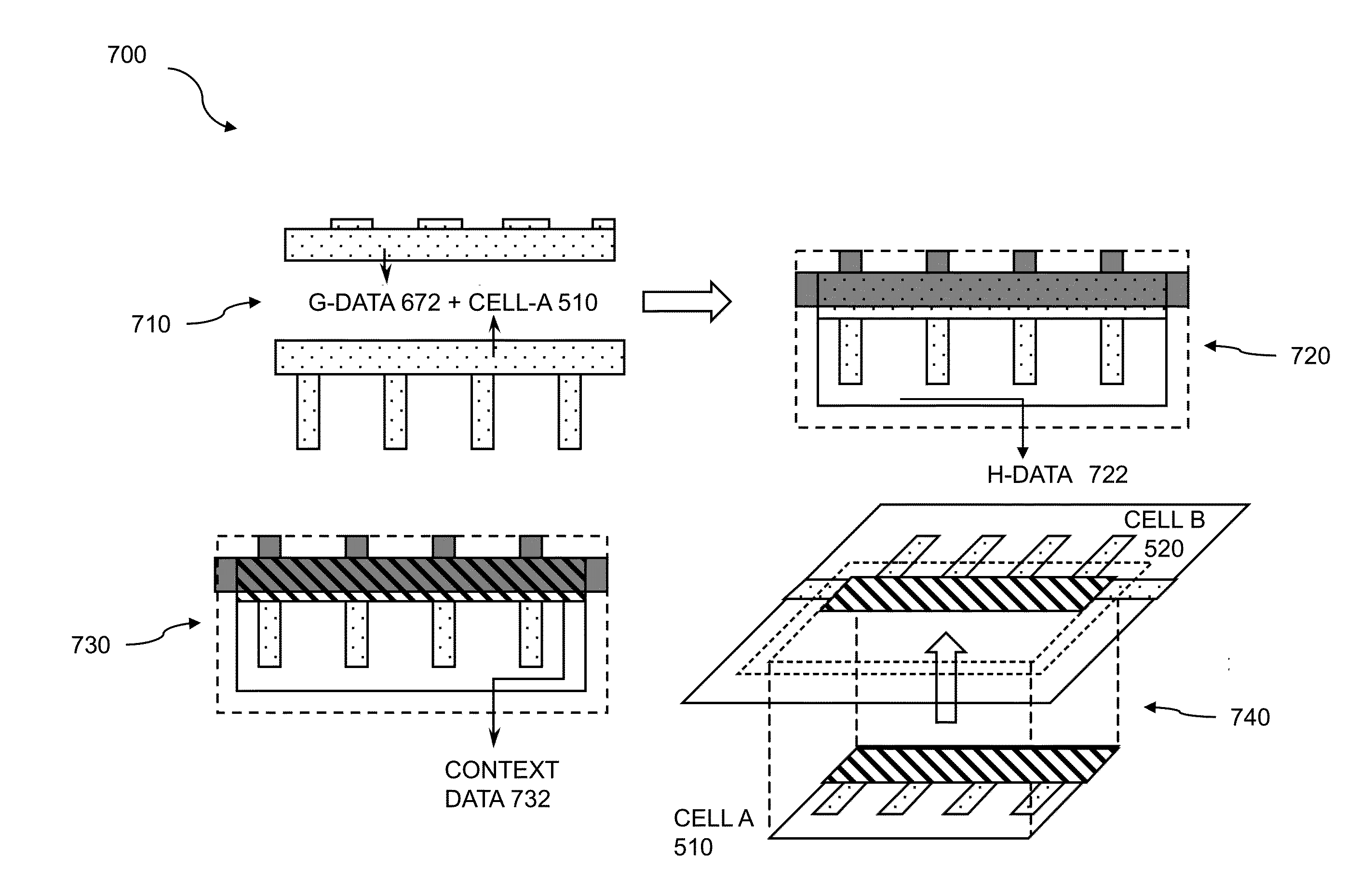
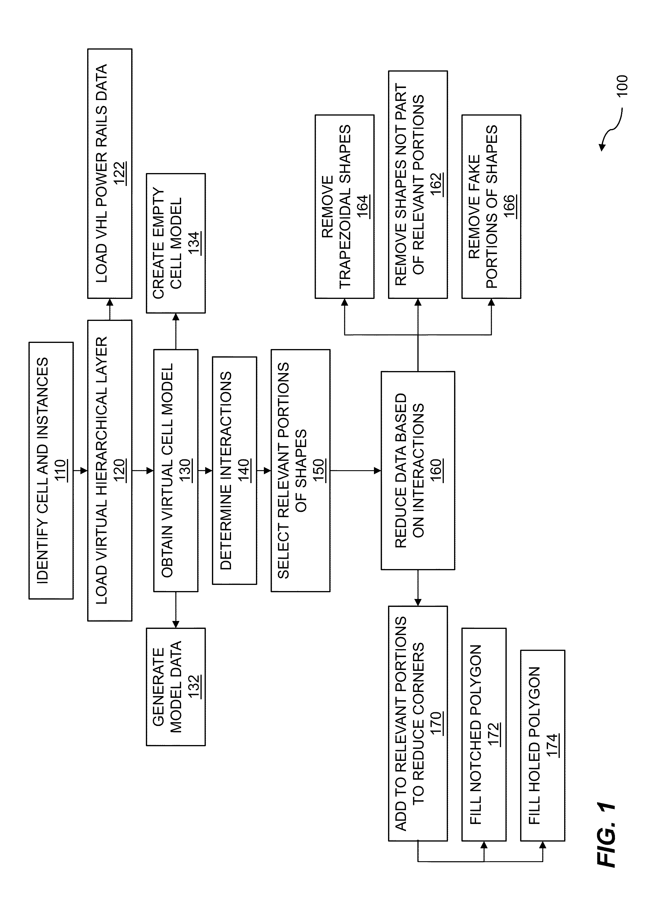
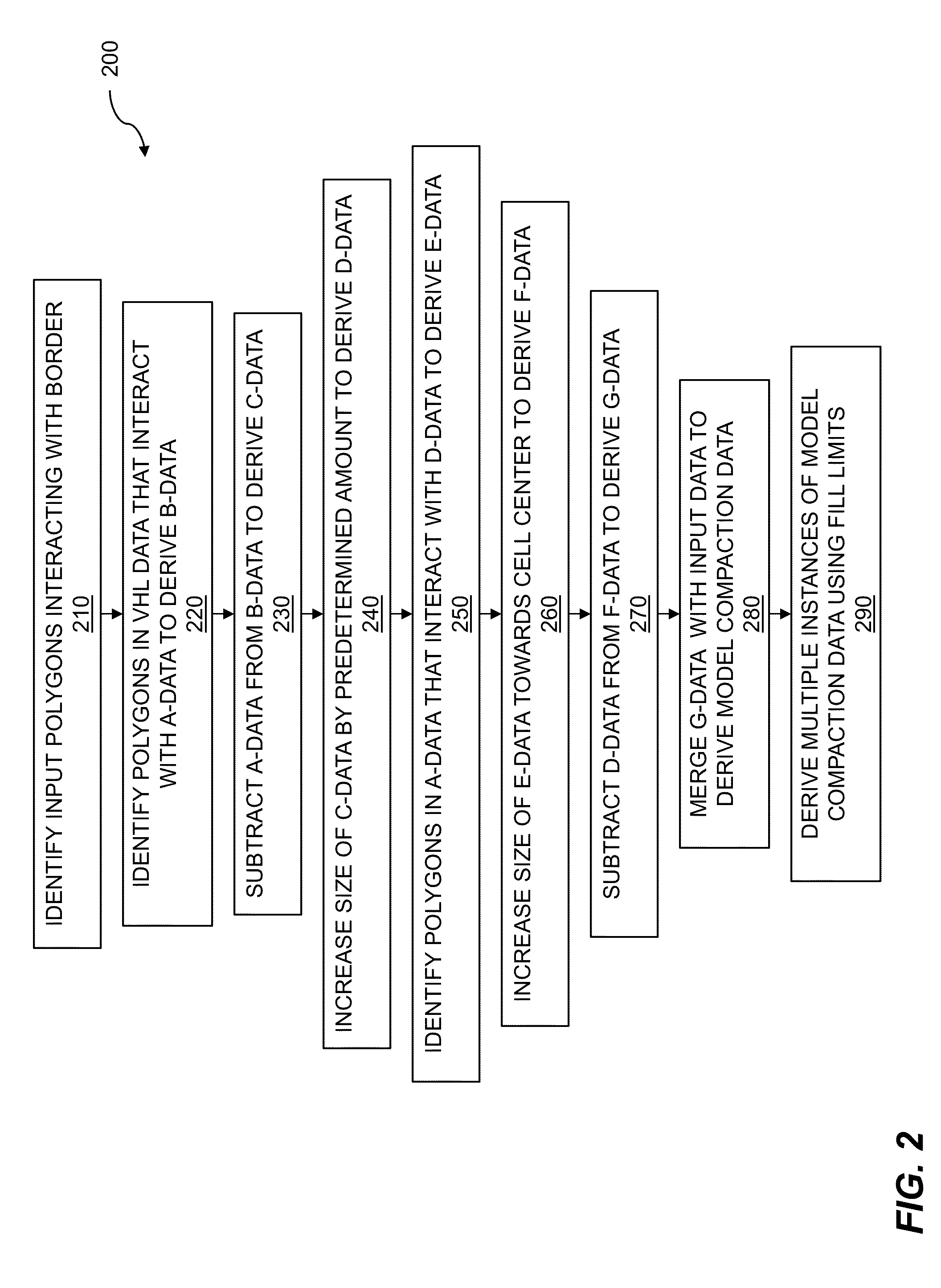
[0022]Methods, systems, and computer program products are described herein that relate to electronic design automation (EDA) and physical verification of semiconductor designs using a design rule checking (DRC) process defined by a semiconductor foundry. More specifically, optimizations related to virtual cell models known as a virtual hierarchical layer (VHL) are described. Embodiments of the present disclosure use a variety of techniques, including, but not limited to, removing area and adding area to the geometric shapes of the VHL to reduce the number of corners in the geometric shapes and thereby reduce the size of the data needed to describe those shapes. The corner reduction effectively acts as a compression of the VHL data, reducing the size of the VHL, which in turn can reduce the memory footprint and computational resources required for the DRC process.

[0023]Hierarchical physical verification of an integrated circuit (IC) is a complex process due in p...


PUM


Abstract

Semiconductor designs are large and complex, typically consisting of numerous circuits called cells. To handle complexity, hierarchical structures are imposed on the semiconductor design to help accomplish analysis, simulation, verification, and so on. The hierarchical structures define architecture, behavior, function, structure, etc. of the semiconductor design. Virtual cells are constructed to compress cell geometries and ease the various design tasks. A cell and multiple instances of the cell are identified within the semiconductor design and the virtual hierarchical levels describing the design. Virtual hierarchical layer (VHL) data based on the cell is loaded. A virtual cell model representative of the cell is obtained. Interactions between cell data and VHL data are determined, and relevant portions of shapes are selected. Data within the virtual cell model is reduced based on the determined interactions.

Description

RELATED APPLICATIONS[0001]This application claims the benefit of U.S. provisional patent applications “Virtual Hierarchical Layer Usage” Ser. No. 62 / 002,808, filed May 24, 2014, “Virtual Hierarchical Layer Patterning” Ser. No. 62 / 006,069, filed May 31, 2014, “Virtual Cell Model Geometry Compression” Ser. No. 62 / 006,657, filed Jun. 2, 2014, “Negative Plane Usage with a Virtual Hierarchical Layer” Ser. No. 62 / 006,083, filed May 31, 2014, “Virtual Cell Model Usage” Ser. No. 62 / 006,607, filed Jun. 2, 2014, and “Virtual Hierarchical Layer Propagation” Ser. No. 62 / 006,092, filed May 31, 2014. Each of the foregoing applications are hereby incorporated by reference in their entirety.FIELD OF ART[0002]This application relates generally to semiconductor circuit design and more particularly to physical verification of semiconductor designs using Design Rule Checking (DRC).BACKGROUND[0003]Electronic products rely on integrated circuits (ICs) which can contain many millions or even billons of tr...

Claims


Application Information

Patent Timeline
IPC IPC(8): G06F17/50
CPCG06F17/5081G06F30/392G06F30/398G06F2119/18Y02P90/02G06F30/00G06F30/20G06F30/39
Inventor NANCE, JAMES LEWISCHEN, JUNNIFONG, GARY B.
Owner SYNOPSYS INC
Why Eureka
Try Eureka